
قدرة النماذج الأولية لثنائي الفينيل متعدد الكلور من UGPCB: الابتكار التكنولوجي & معيار الصناعة وراء التسليم السريع خلال 72 ساعة
ثنائي الفينيل متعدد الكلور (لوحة الدوائر المطبوعة) serves as the “skeleton” and “nervous system” of modern electronics, بمثابة الناقل الأساسي الذي يربط جميع المكونات الإلكترونية. من الهواتف الذكية إلى الاتصالات عبر الأقمار الصناعية, الأجهزة الطبية لأنظمة القيادة الذاتية, زيادة 99% تعتمد الأجهزة الإلكترونية على التشغيل المستقر لمركبات ثنائي الفينيل متعدد الكلور عالية الأداء. في المنافسة الشرسة لتطوير المنتجات, سريع, موثوق, وعالية الجودة خدمات النماذج الأولية لثنائي الفينيل متعدد الكلور أصبحت عاملا حاسما للشركات التي تهدف إلى اغتنام الفرص المتاحة في السوق. الاستفادة من الخبرة التقنية العميقة ونظام التصنيع المتقدم, UGPCB هو إعادة تعريف معايير الصناعة ل انعطاف سريع تصنيع ثنائي الفينيل متعدد الكلور.
🔍 أنا. النماذج الأولية لثنائي الفينيل متعدد الكلور: حجر الزاوية واختبار عباد الشمس للابتكار الإلكتروني
يمتد تطور مركبات ثنائي الفينيل متعدد الكلور 130 سنين. من الأسلاك اليدوية المبكرة إلى اليوم ربط عالية الكثافة (مؤشر التنمية البشرية) و ركائز IC, وقد تقدم تطورها بالتزامن مع ثورات التكنولوجيا الإلكترونية. التطبيق العملي ل صفح مكسو بالنحاس (سي سي إل) كانت التكنولوجيا خلال الحرب العالمية الثانية نقطة تحول محورية, استبدال لحام الأسلاك اليدوي المعقد والمعرض للأخطاء ووضع الأساس للموثوقية, استقرار, وتصغير الإلكترونيات الحديثة.
-
تحدي المهندس: إن الالتزام بتصميم ثنائي الفينيل متعدد الكلور مع وجود عيوب لم يتم حلها في الإنتاج الضخم يؤدي إلى عواقب كارثية - فشل في الأداء, يتذكر مكلفة, تأخير المشروع, خسارة العملاء, والإضرار بسمعة العلامة التجارية.
-
حل UGPCB: تقديم شامل, عالية الدقة, والاستجابة السريعة تصميم ثنائي الفينيل متعدد الكلور و خدمات النماذج الأولية لثنائي الفينيل متعدد الكلور هي الضمانة الأولى والأكثر أهمية للمهندسين الذين يقومون بتحويل المفاهيم المبتكرة إلى منتجات موثوقة.
-
💡 البصيرة المهنية: القيمة الأساسية ل النماذج الأولية لثنائي الفينيل متعدد الكلور lies in “early detection, early correction.” Statistics show that fixing errors during the prototype phase costs merely 1/100th (أو أقل) من التكلفة المتكبدة أثناء الإنتاج الضخم. UGPCB النماذج الأولية السريعة لثنائي الفينيل متعدد الكلور القدرة هي المفتاح لإنقاذ العملاء بشكل كبير R&د- التكاليف والوقت.
🛠️ثانيا. الغوص العميق: القدرات الفنية الأساسية لـ UGPCB في النماذج الأولية لثنائي الفينيل متعدد الكلور
تغطي قدرات التصنيع لدى UGPCB كل شيء بدءًا من اللوحات الأساسية أحادية/مزدوجة الجانب وحتى اللوحات المتطورة ركائز التعبئة والتغليف IC, تتميز بمعايير صارمة وعمليات رائدة في الصناعة.
📊 1. معلمات العملية الأساسية & المواصفات الفنية (نظرة عامة على قدرات النماذج الأولية لـ UGPCB)
-
البيانات الرئيسية:
-
نطاق سمك اللوحة: مفردة/مزدوجة: 0.10mm – 8.0mm (4 mil – 315 ميل); متعدد الطبقات: 0.15mm – 8.0mm (6 mil – 315 ميل)
-
دقيقة. الحجم النهائي: 0.5 × 1.0 ملم (القدرة على التصغير الشديد)
-
الأعلى. طبقات: معيار: حتى 100 طبقات (يتطلب المراجعة); الترددات اللاسلكية الهجينة: 4-32 طبقات
-
عالية التردد / خاص مواد: روجرز®, آرلون®, تاكونيك®, ايزولا® (FR408, 370الموارد البشرية), تفلون®/PTFE, سيراميك, السيراميك الهيدروكربوني, المواد الهجينة
-
📡 2. عالية التردد & النماذج الأولية لثنائي الفينيل متعدد الكلور عالي السرعة: مفتاح السيطرة على عصر جيجاهيرتز
مدفوعة بالزيادة في 5G / 6G, رادار, الاتصالات عبر الأقمار الصناعية (الترددات >1GHz), ومتطلبات حوسبة الذكاء الاصطناعي, مركبات ثنائي الفينيل متعدد الكلور عالية السرعة عالية التردد هي أرض تكنولوجية عالية. يكمن التحدي الأساسي في التحكم في فقدان الإشارة والحفاظ على استقرار المعاوقة.
-
التحديات التقنية: استقرار ثابت العزل الكهربائي (DK) & خسارة الظل (ص), خشونة سطح رقائق النحاس, التحكم الدقيق في سمك الطبقة العازلة.
-
مزايا UGPCB:
-
الخبرة المادية: معالجة مثبتة للأعلى شرائح عالية التردد مثل روجرز® (™3000 ريال عماني, سلسلة RO4000®), آرلون® (سلسلة AD/CL), تاكونيك® (آر إف-35, سلسلة TLY), ايزولا® (FR408HR, أسترا™).
-
السيطرة على المعاوقة: رقابة صارمة على التسامح في حدود ± 5%, غالبا ±3%, تلبية الأكثر تطلبا سلامة الإشارة متطلبات.
-
التطبيقات: رادار الموجة المليمترية, حمولات الاتصالات عبر الأقمار الصناعية, معدات الشبكات عالية السرعة (400جم/800 جم), أدوات الاختبار الراقية.
-
-
📐 Technical Formula – Characteristic Impedance (نموذج مبسط للشرائح الدقيقة):
Z₀ ≈ (87 / √(εr + 1.41)) * ln(5.98h / (0.8w + t))-
Z₀: مقاومة الهدف (أوه) -
εr: مادة الركيزة ثابت العزل الكهربائي النسبي -
h: سمك العزل الكهربائي (ميل) -
w: عرض التتبع (ميل) -
t: تتبع سمك (ميل) -
يستخدم مهندسو UGPCB حسابات ومحاكاة دقيقة لضمان ذلك مقاومة الدائرة عالية التردد يطابق بدقة قيم التصميم.
-
🔄 3. النماذج الأولية لثنائي الفينيل متعدد الكلور الصلب المرن: التمكين المثالي للتصاميم ثلاثية الأبعاد المعقدة
مركبات ثنائي الفينيل متعدد الكلور الصلبة المرنة تجمع بين الدعم المستقر للألواح الصلبة مع قدرة الانحناء الديناميكي للدوائر المرنة, تقديم حل ثوري لتصغير الجهاز, تخفيض الوزن, وتعزيز الموثوقية.
-
المزايا الفريدة:
-
يقلل بشكل كبير من الموصلات والكابلات, تحسين موثوقية النظام (نقاط فشل أقل).
-
يتكيف بحرية مع المساحات ثلاثية الأبعاد المعقدة, تحسين تخطيط الجهاز الداخلي.
-
يقلل من الوزن والحجم الإجمالي, مثالية ل الأجهزة القابلة للارتداء, الفضاء الجوي, و الأدوات الطبية الدقيقة.
-
-
التحديات & اختراقات UGPCB:
-
نقاط الألم التقليدية: العمليات المعقدة (ما يصل الى 50+ خطوات), تكاليف مادية عالية, صعوبات التحكم في العائد, دورات الإنتاج الطويلة.
-
حل UGPCB: تحسين اختيار المواد (على سبيل المثال, غطاء PI/مطابقة لاصقة), باستخدام التصفيح عالي الدقة والحفر بالليزر, تنفيذ رقابة صارمة على العملية (لكل IPC-2223B, 6013معايير د), تعزيز العائد بشكل فعال وتقصير فترات زمنية النموذج الأولي.
-
🧩 4. مركبات ثنائي الفينيل متعدد الكلور ذات طبقة عالية & النماذج الأولية لركيزة IC: تمكين التكامل عالي الكثافة
تعمل الإلكترونيات القوية بشكل متزايد على دفع مركبات ثنائي الفينيل متعدد الكلور نحوها عدد طبقات عالية (>10 طبقات), توجيه عالي الكثافة, والتغليف المتقدم. ركائز IC, acting as the “interpreter” between chips and motherboards, تقديم حواجز تقنية عالية للغاية.
-
اتجاهات متعددة الطبقات: تقليص عرض/مساحة الخط بشكل مستمر (L/S وصولاً إلى ≥50μm/50μm), دقة أعلى للميكروفياس (<100ميكرومتر), محاذاة أكثر صرامة من طبقة إلى طبقة.
-
IC Substrate – The Core of Packaging:
-
تعريف: مركبات ثنائي الفينيل متعدد الكلور المتطورة تقوم بتركيب الشريحة مباشرة (يموت), توفير الربط الكهربائي, الإدارة الحرارية, والحماية الجسدية.
-
الخصائص الرئيسية: توجيه عالي الكثافة (تقنية HDI/SLP), النوى رقيقة جدا (<100مم ممكن), الخطوط الدقيقة (L/S يصل إلى 20μm/20μm), ارتفاع سطح التسطيح, إدارة حرارية ممتازة.
-
قوة UGPCB: تمتلك ناضجة بغا (مصفوفة شبكة الكرة) و eMMC (بطاقة الوسائط المتعددة المدمجة) الركيزة النماذج الأولية وقدرات الإنتاج ذات الحجم المنخفض إلى المتوسط, دعم العميل ر&د في المعالجات, ذاكرة, رقائق تسريع الذكاء الاصطناعي, وأكثر.
-
⏱️ثالثا. سرعة & ميزة التكلفة: القدرة التنافسية الأساسية لـ UGPCB في النماذج الأولية لثنائي الفينيل متعدد الكلور
In the electronics market where “speed is paramount,” prototyping velocity directly impacts وقت الوصول إلى السوق (تم). معًا, يعد التحكم الفعال في التكلفة أمرًا بالغ الأهمية بالنسبة لـ R&د- الميزانيات.
-
التسليم السريع: يعمل UGPCB على تحسين تدفق الإنتاج وإدارة سلسلة التوريد. المهل الزمنية القياسية لنموذج ثنائي الفينيل متعدد الكلور يمكن ضغطها بشكل مثير للإعجاب 72 ساعات (3 أيام). لوحات معقدة (على سبيل المثال, RF, مؤشر التنمية البشرية, جامدة فليكس, >20 طبقات) عادة ما تكون كاملة داخل 1-2 أسابيع (اعتمادا على التعقيد), تتجاوز بكثير متوسطات الصناعة.
-
استراتيجية النماذج الأولية منخفضة التكلفة:
-
التحقق من صحة التصميم الفعال: يستخدم مواد فعالة من حيث التكلفة وعمليات موحدة للتحقق الوظيفي السريع.
-
حلول مرنة: يوصي بمجموعات المواد والعمليات الأكثر فعالية من حيث التكلفة بناءً على احتياجات الاختبار (الأداء الكهربائي, تناسب ميكانيكي, الوظيفة الأساسية).
-
عرض القيمة: التحقق المبكر من صحة النموذج الأولي يمكن أن يمنع ما يصل إلى 90% من الخسائر المحتملة أثناء الإنتاج الضخم. UGPCB النماذج الأولية لثنائي الفينيل متعدد الكلور منخفضة التكلفة هو الاختيار الذكي لإدارة R&د خطر.
-
📌 دعوة للعمل: السعي خدمات النماذج الأولية لثنائي الفينيل متعدد الكلور التي تجمع بين السرعة, مصداقية, وميزة التكلفة? اتصل بـ UGPCB الآن للحصول على عرض أسعار مخصص! نحن نقدم سوق دبي المالي مجاني (تصميم للتصنيع) تحليل لتحسين التصميم الخاص بك وتسريع إطلاق المنتج! [انقر فوق أداة الدردشة المباشرة في أسفل اليمين للحصول على دعم فني مجاني]
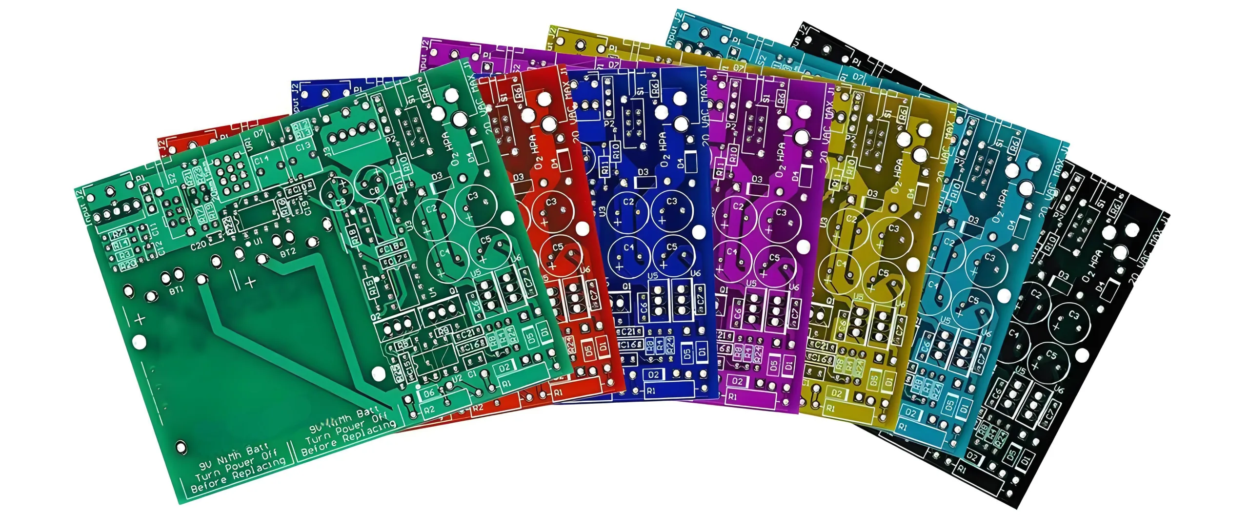
🎨رابعا. ما وراء الأخضر: علم وفن اختيار ألوان ثنائي الفينيل متعدد الكلور
While “engineering green” is the classic PCB look, ألوان قناع اللحام تقديم المزيد من التنوع. يوفر UGPCB خيارات مثل اللون الأزرق, أصفر, أحمر, أسود, والأبيض – ليس فقط بسبب الجماليات, ولكن أيضًا الوظيفة:
-
ثنائي الفينيل متعدد الكلور الأبيض: انعكاسية عالية, يعزز بشكل كبير كفاءة الضوء والتوحيد في تطبيقات الإضاءة LED.
-
ثنائي الفينيل متعدد الكلور الأسود: انعكاسية منخفضة, يقلل من تداخل الضوء الشارد, مثالية لمعدات المسرح, منتجات AV المتطورة, نقل إحساس احترافي بسيط.
-
تقتيش & إعادة صياغة: تباين عالي بين الخلفيات الفاتحة (أصفر, أبيض) وآثار داكنة (أخضر, أزرق) يسهل الفحص البصري والإصلاح اليدوي.
-
هوية العلامة التجارية: تعمل الألوان المخصصة على تعزيز الهوية البصرية للمنتج صورة العلامة التجارية.

🚀V. من التصميم إلى الإنتاج الضخم: حلقة قيمة حل PCB الشامل من UGPCB
تمتد قيمة UGPCB إلى ما هو أبعد من تصنيع الألواح العارية, تشمل دورة حياة المنتج بأكملها:
-
دعم التصميم & التحقق من صحة النموذج الأولي (القيمة الأساسية): النماذج الأولية السريعة يوفر النافذة الذهبية للعثور على عيوب التصميم وإصلاحها, ضمان أساس قوي.
-
وظيفة & اختبار الأداء: يستخدم المهندسون النماذج الأولية ل سلامة الإشارة (و), سلامة السلطة (باي), المحاكاة الحرارية, اختبار الإجهاد البيئي, إلخ., التحقق من أداء المنتج في ظل ظروف مختلفة.
-
تسويق & القوة التجريبية: وظيفية بالكامل ثنائي الفينيل متعدد الكلور النماذج الأولية مثالية للمعارض, عروض العميل, وملاعب التمويل, عرض قيمة المنتج بشكل ملموس.
-
منحدر سلس للإنتاج: تتوافق عمليات النماذج الأولية في UGPCB بشكل وثيق مع خطوط الإنتاج الضخم, ضمان الأداء المتسق وتخفيف مخاطر التحول.
-
ثنائي الفينيل متعدد الكلور (حَشد) خدمات النماذج الأولية: العروض كاملة النماذج الأولية لـ PCBA مشتمل مصادر المكونات (بوم), تجميع سمت, تي إتش تي (تراجع) حَشد, والاختبار. يؤدي تقديم وحدات وظيفية جاهزة للتشغيل إلى تسريع عملية تطوير المنتج النهائي بشكل كبير يختصر وقت الوصول إلى السوق.
💎الخلاصة: اختر UGPCB, اختر مسرع الابتكار
في صناعة الإلكترونيات سريعة الخطى, الوقت هو حصة السوق, والجودة أمر بالغ الأهمية. UGPCB, معها:
-
قدرات عملية متطورة (تغطي الترددات اللاسلكية/عالية السرعة, جامدة فليكس, عدد طبقات عالية, ركائز IC),
-
سرعة التسليم القصوى (الأسرع 72 ساعات),
-
استراتيجيات التكلفة المرنة (خيارات التحقق منخفضة التكلفة),
-
أنظمة الجودة الصارمة (الامتثال ل IPC, إلخ.),
-
سلسلة خدمات شاملة (دعم التصميم, النماذج الأولية لثنائي الفينيل متعدد الكلور, تجميع PCBA),
أصبح الموثوق به نموذج ثنائي الفينيل متعدد الكلور وشريك التصنيع الحجمي للمهندسين العالميين و R&فرق د. سواء في مجال الالكترونيات الاستهلاكية, إلكترونيات السيارات, الأجهزة الطبية, التحكم الصناعي, الفضاء الجوي, أو الاتصالات, يوفر UGPCB مادة صلبة, سريع, وأساس مادي عالي الجودة لابتكارك.
اتخذ إجراءً الآن!
-
احصل على عرض أسعار النموذج الأولي لثنائي الفينيل متعدد الكلور المخصص لك
-
استشارة خبير: فريقنا الفني جاهز للإجابة على أسئلتك تصميم عالي التردد, الهياكل الصلبة المرنة, التحكم في المعاوقة, اختيار المواد, وأكثر.
-
اكتشف المزيد من القدرات:
اختر UGPCB – فلنكن شريكك القوي على طريق النجاح!