

Revolutionary Breakthrough in Flexible Electronics
In the graceful folds of smartphone displays and the precise movements of Mars rover arms, لوحات الدوائر المطبوعة مرنة (FPCBS) يقودون بهدوء الثورة الثالثة في الإلكترونيات. According to Prismark data, the global FPCB market surpassed $120 مليار في 2023, with a compound annual growth rate (CAGR) ل 8.7%. This innovative technology, combining conductors with flexible dielectric films, is redefining the physical form and functional boundaries of electronic devices.
أنا. The Taxonomy of Flexible Circuits
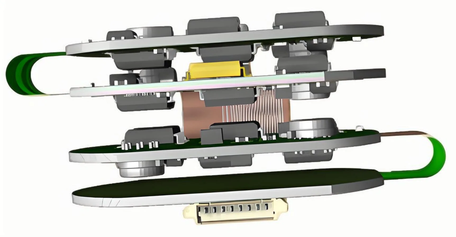
1.1 The Art of Rigid-Flex Harmony
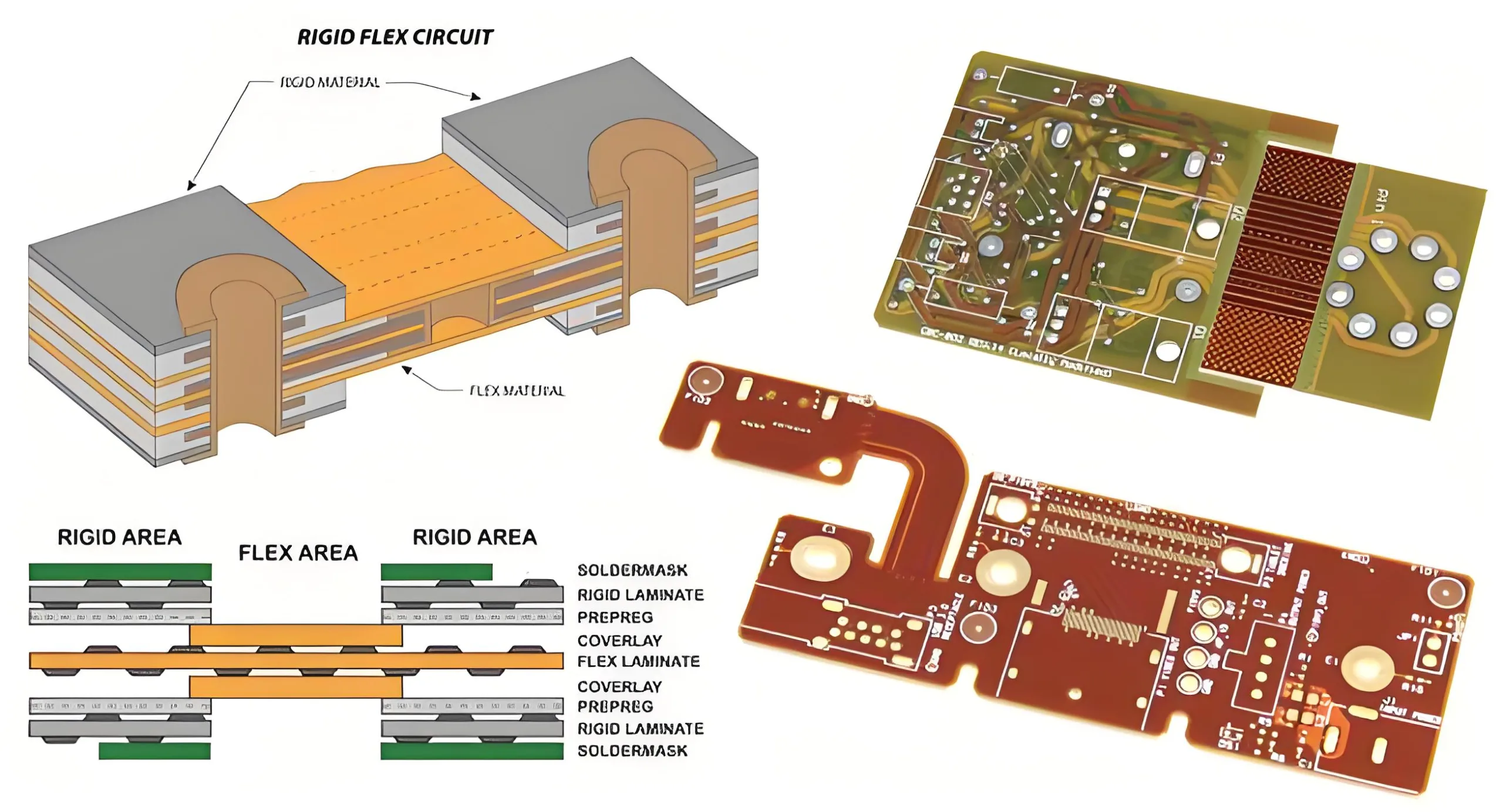

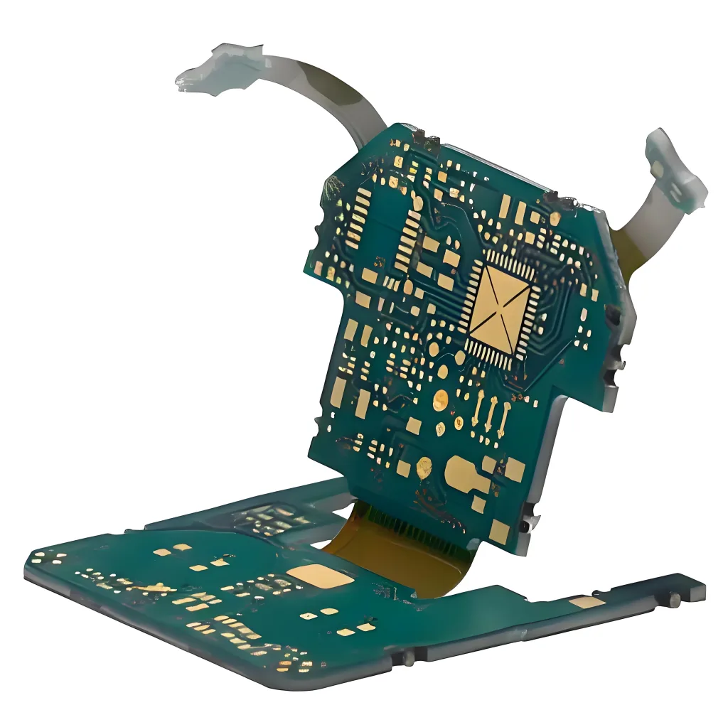
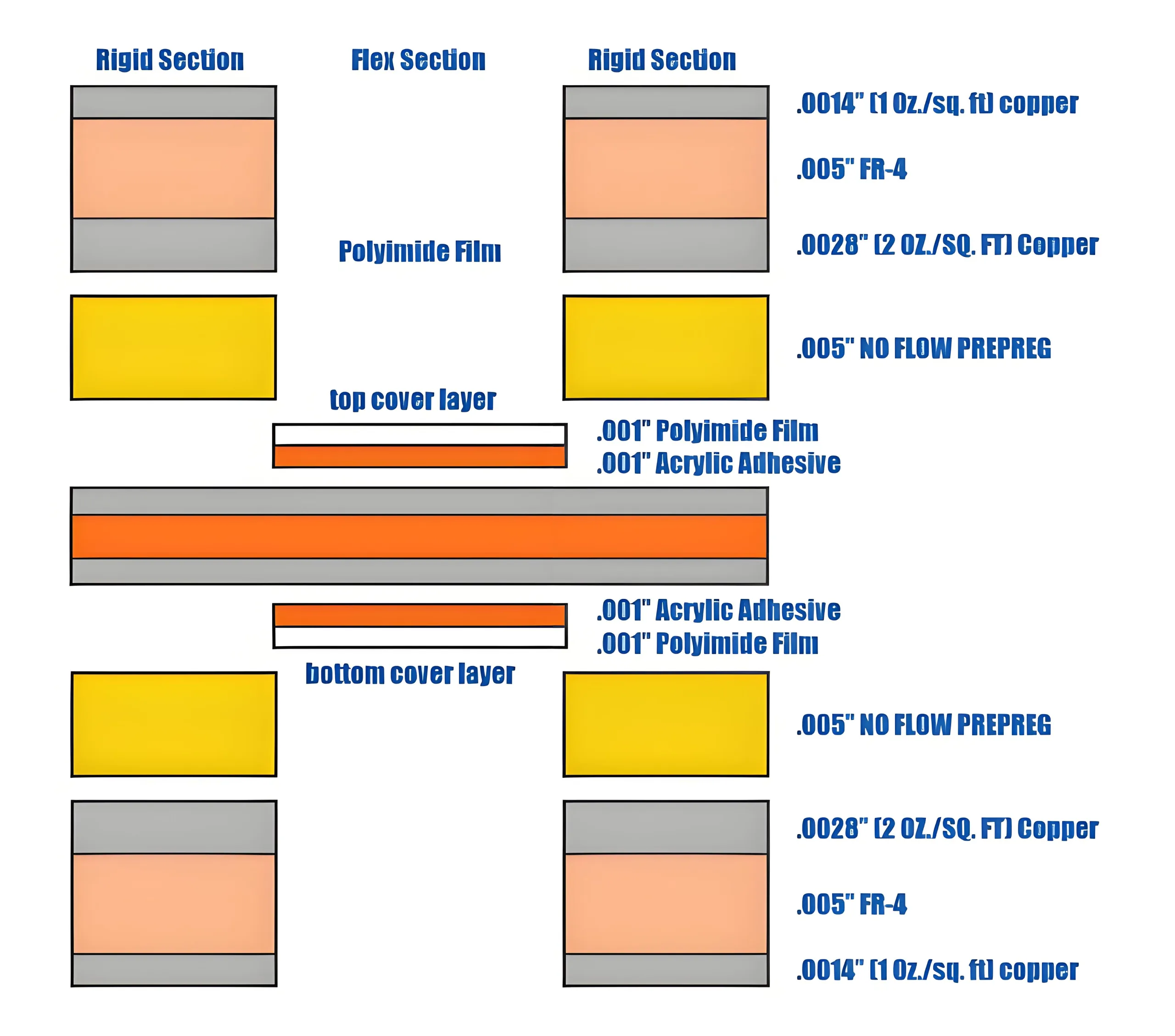
Flexible circuits fall into two categories: pure flexible circuits (الشركة العامة للفوسفات) and rigid-flex hybrids. The former, as thin as cicada wings (0.1–0.3 mm), employs flexible plastic substrates, while the latter fuses rigid FR4 sections with polyimide flexible zones using epoxy resins. In smartphones, rigid-flex designs enable a bending radius as small as 3 مم (صيغة: R_min = 100×t, أين ر = material thickness), seamlessly connecting mainboards to displays.
1.2 Strategic Selection Between Static and Dynamic Applications
- Static Applications: Automotive dashboard circuits (<100 annual bends) use 3-layer rolled copper structures with 18μm foil.
- Dynamic Applications: Laptop hinge circuits require >1 million bend cycles, demanding 2-layer electrodeposited copper with steel reinforcement.

ثانيا. The Precision Game of Material Science
2.1 Evolution of Substrate Materials
Polyimide (باي) films dominate high-end applications with a glass transition temperature (تيراغرام) of 260°C and elastic modulus of 16 GPa. Emerging liquid crystal polymer (LCP) مواد, featuring 0.2% moisture absorption and >10 GHz high-frequency performance, are revolutionizing 5G mmWave applications.
2.2 The Micron-Scale Battle of Copper Foils
The choice between rolled annealed (RA) and electrodeposited (ED) copper foils involves critical trade-offs:
- RA Foil: 20% elongation for dynamic bending
- ED Foil: 30% cost reduction for static use
XRD analysis reveals RA foil’s (220) crystal plane orientation reaches 85%, explaining its exceptional ductility.
ثالثا. Multidimensional Design Strategies
3.1 Stackup Topology Optimization
In autonomous radar modules, engineers adopt a “2-2-2” stackup: 6-layer routing in rigid zones and retained L2/L5 signal layers in flexible areas. This limits dielectric constant variation to ±5% in bend zones, ضمان 77 GHz signal integrity.

3.2 Digital Twin of Bend Mechanics
Finite element analysis (FEA) models bending stress using:
σ_max = (E×t)/(2ر)
أين E = elastic modulus, ر = thickness, ر = bend radius. Copper strain exceeding 0.3% triggers reinforcement or routing optimizations.
رابعا. Breaking Manufacturing Boundaries
4.1 The Art of 3D Folding
ANSYS Mechanical multiphysics simulations must account for:
- Mechanical stress distribution
- CTE matching (PI material CTE ≈15 ppm/°C)
- High-frequency phase stability
4.2 Golden Rules of Design for Manufacturing
- No vias in bend zones (clearance >3 مم)
- “10-Degree Rule” for conductor angles between adjacent layers
- Coverlay opening formula: D_pad = D_solder + 0.1 مم

V. Future Frontiers: The New Horizon of Flexible Electronics
In metaverse devices, FPCBs transcend traditional forms. MIT’s 3D-printed circuits achieve 500% tensile deformation, while Stanford’s biodegradable variants show promise in implantable medical tech. With roll-to-roll (R2R) manufacturing cutting costs by 8% annually, a fully flexible intelligent era dawns.
Epilogue: Balancing Rigidity and Flexibility for Tomorrow
From Apollo lunar modules to foldable smartphones, FPCBs have evolved over 60 years from aerospace marvels to daily essentials. Engraving circuits on 0.1mm polyimide films writes an industrial epic at microscopic scales. This dynamic field awaits engineers to redraw electronics’ future along the philosophical boundary between rigidity and flexibility.