

في التجمع SMT, يمكن أن يؤدي وجود خلل على نطاق ميكرون إلى الإضرار بالجودة. ل ثنائي الفينيل متعدد الكلور designers and ثنائي الفينيل متعدد الكلور production managers, كرات لحام ثابتة على منصات مكونات الرقاقة (مثل المقاومات والمكثفات MLCC) هي قضية مشتركة. These defects affect aesthetics and can cause short circuits in demanding applications, threatening product reliability. This guide analyzes the five root causes of solder balls and provides a systematic, IPC-based solution framework to enhance soldering yield.

The Core Mechanism: Paste Squeeze and Failed Containment
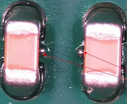
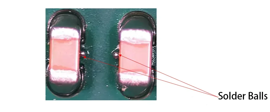
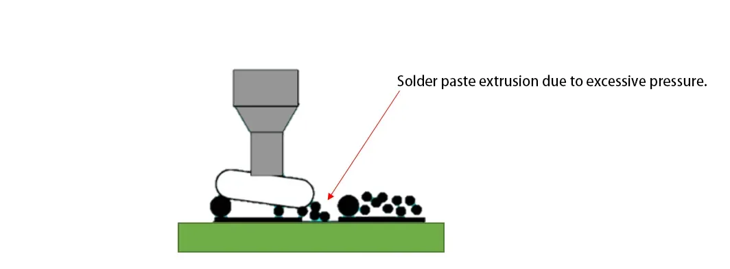
Solder balls “escape” rather than “form.” During reflow, molten solder paste fails to coalesce into the main joint due to surface tension, separating and balling up at the pad edges. Per IPC-A-610, a solder ball is a defect if its diameter exceeds 0.13mm or if it risks bridging conductors.
The primary cause is solder paste being squeezed onto the solder mask during printing or placement. The non-wettable solder mask prevents paste from rejoining the main joint, forming independent balls.
Root Cause 1: PCB Design “Topography”
تصميم ثنائي الفينيل متعدد الكلور is the first defense. Poor pad and solder mask design creates escape routes.
1. Solder Mask Dams: To Keep or Remove?
Traditional solder mask dams between adjacent Chip pads prevent bridging but create paste-trapping trenches. Removing the dam eliminates this terrain, allowing paste to deposit cleanly on the pad for unified surface tension control during reflow.
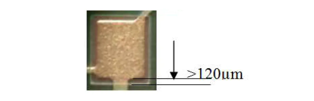
2. Solder Mask Opening (مصلحة الارصاد الجوية): Ensure Adequate Buffer
The SMD must be larger than the copper pad. IPC-7351 recommends a minimum 75µm (3ميل) single-side gap for Chip components, with 120µm (5ميل) as best practice. This buffer accommodates minor solder mask misalignment, ensuring paste contacts only the wettable copper.

3. Manage Manufacturing Tolerances
Collaborate with your PCB supplier. Specify stringent solder mask alignment tolerances (typically ≤50µm) and choose a supplier capable of meeting them within your design’s buffer zone.
Root Cause 2: Stencil Design “Dosage Control”
ال stencil dictates paste volume and shape.
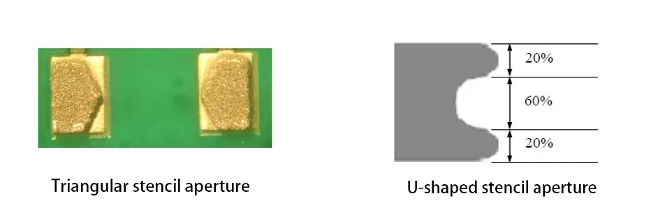
1. Volume Reduction & Shaping: U-Shaped/Triangular Apertures
ل 0402 and larger components, reduce paste volume. Advanced designs use U-shaped or triangular apertures instead of squares. This reduces center volume while directing paste to the pad ends, providing sufficient solder while minimizing squeeze-out. This can reduce paste volume by 15-20%.
2. Optimize Aperture Ratio
Stencil aperture width is typically 80-90% of the pad width. Ensure an Area Ratio > 0.66 for clean release and precise volume control.

Root Cause 3: Pursuing “Zero Gap” in Paste Printing
Printing defines initial paste placement.
1. Achieve True Zero-Gap Contact
Any stencil-PCB gap causes paste bleed under squeegee pressure. Ensure a flat support platform and optimal pin placement for uniform PCB backing. Calibrate machine parallelism regularly.
2. Maintain Cleaning and Alignment
Dried paste on the stencil bottom creates gaps. Implement frequent bottom-side wiping (على سبيل المثال, كل 5-10 boards for fine-pitch components). Use high-precision vision alignment for perfect stencil-to-pad registration.
Root Cause 4: “Gentle” Component Placement
Placement can crush paste.
Excessive Z-force or low placement height squeezes paste out. Set the component placement height ل 1/2 ل 2/3 of the post-print paste height. This allows the part to “kiss” the paste without impact.

Root Cause 5: Reflow “Thermodynamic” Control
The reflow profile, especially preheat, is critical.
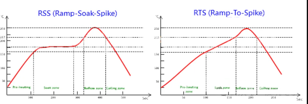
1. Avoid Extended Preheat and “Hot Slump”
Long soak zones can cause “hot slump”: premature flux evaporation/viscosity drop makes paste slump and spread onto the solder mask before melting, leading to ball formation.
2. Use a Ramp-to-Peak or Linear Profile
Shorten or eliminate the soak plateau. Use a controlled linear ramp from ambient to peak, with a preheat rate of 1.0-2.0°C/sec. This reduces low-temperature dwell time, limits slump, and allows synchronous melting for effective surface tension pull.
Data Point: Per IPC/JEDEC J-STD-020, for SAC305 solder, هدف 60-90 seconds above liquidus (TAL) and a 235-245°C peak. Optimize the preheat slope within these constraints.

خاتمة: A Systemic Optimization Approach
Solving Chip component solder balls requires a system engineering approach across تصميم ثنائي الفينيل متعدد الكلور, stencil fabrication, SMT printing, component placement, وإنحسر لحام.
Checklist for Solder Ball Reduction:
-
تصميم ثنائي الفينيل متعدد الكلور: Are solder mask dams removed? Are SMD openings ≥120µm?
-
Stencil Design: Are U-shaped/triangular apertures used? Is the aperture ratio correct?
-
Printing Process: Is stencil cleaning frequent? Is alignment accuracy high?
-
Placement Program: Is placement height set to 1/2 – 2/3 of paste height?
-
Reflow Profile: Can you implement a linear ramp with a controlled preheat rate?
For high-reliability products, engage a professional PCBA manufacturer ل تصميم للتصنيع (سوق دبي المالي) review early on. An experienced EMS partner can identify risks and provide proven solutions. Through collaborative design and process control, solder balls can be minimized to within IPC acceptability limits, achieving higher first-pass yield and superior board reliability.