
What is a 12L 2+N+2 HDI PCB?
A 12L 2+N+2 HDI PCB refers to a twelve-layer ربط الكثافة العالية (مؤشر التنمية البشرية) لوحة الدوائر المطبوعة, featuring two core layers flanked by N signal layers and another two core layers. This configuration allows for high density interconnections, making it suitable for advanced electronic applications. The “2+N+2” designation indicates the arrangement of the core and signal layers.

Design Considerations
Designing a 12L 2+N+2 HDI PCB involves several critical factors:
- Layer Stacking: Proper alignment of the core and signal layers to ensure optimal electrical performance.
- Trace and Space: Minimal trace width and space of 3mil/3mil to accommodate fine features.
- Hole Sizes: Mechanical holes as small as 0.2mm and laser holes down to 0.1mm for precise component placement.
- سمك النحاس: Varied copper thickness with inner layers at 1OZ and outer layers at 0.5OZ to balance conductivity and flexibility.
How Does It Work?
The functionality of a 12L 2+N+2 اتش دي اي ثنائي الفينيل متعدد الكلور relies on its multilayer structure and the use of high-density interconnects. Each layer serves a specific purpose:
- Core Layers: Provide structural integrity and act as the foundation for signal layers.
- Signal Layers: Carry electrical signals between components.
- المعالجة السطحية: Immersion gold plus OSP ensures excellent solderability and long-term reliability by preventing oxidation.
Applications and Classifications


Materials and Performance
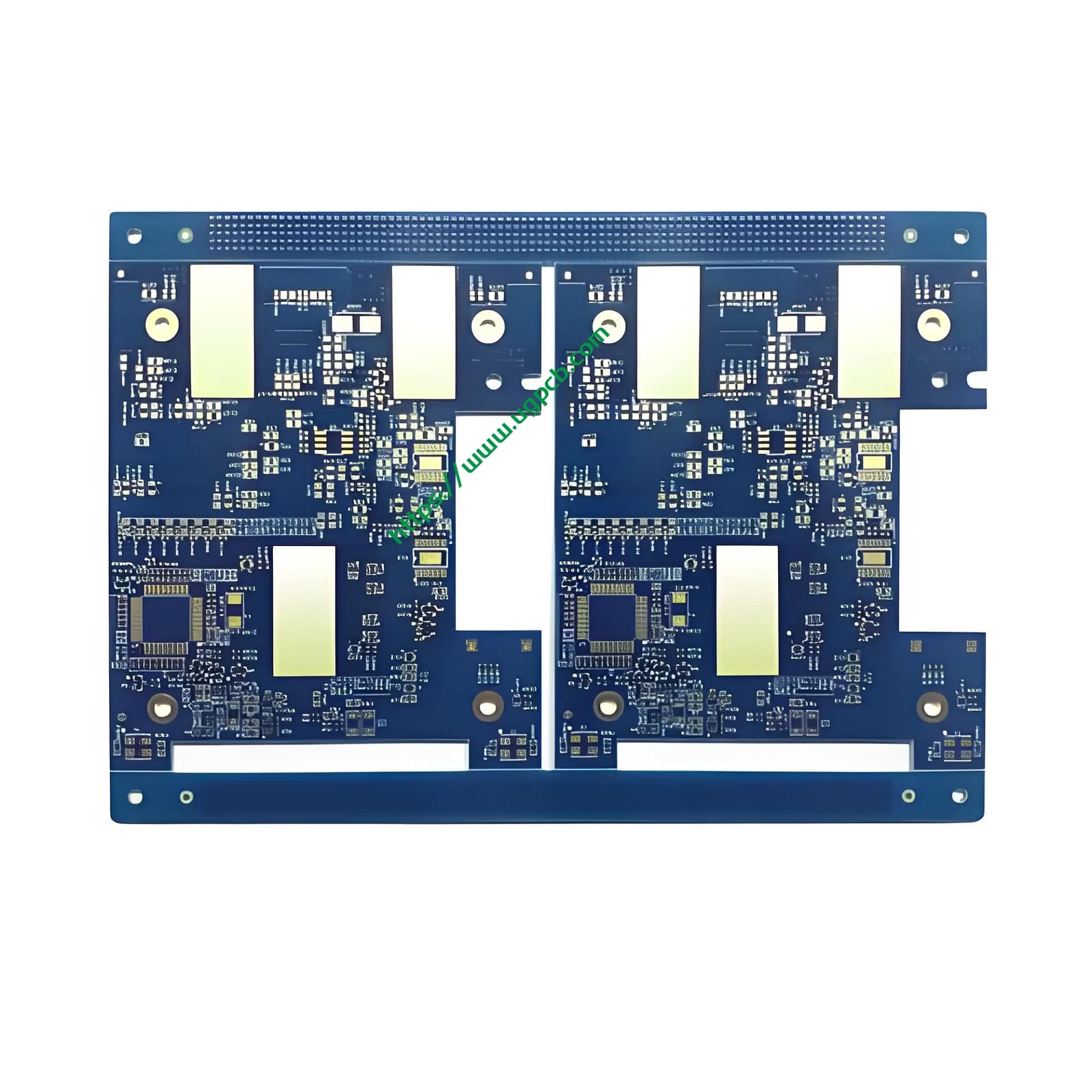
Constructed from FR-4 ITEQ, these PCBs offer excellent thermal stability and mechanical strength. The blue/white color scheme aids in visual inspection and troubleshooting. The finished thickness of 1.6mm provides a robust yet flexible board suitable for intricate designs.
Structure and Features
The unique structure of a 12L 2+N+2 HDI PCB includes:
- Twelve Layers: Two core layers, N signal layers, and another two core layers.
- High Density Interconnects: Allow for complex routing and minimal space usage.
- المعالجة السطحية: Immersion gold plus OSP enhances conductivity and protects against corrosion.
Production Process
The manufacturing process involves several sophisticated steps:
- إعداد المواد: Selecting high-quality FR-4 substrate and copper foils.
- Layer Stacking: Arranging the layers in a precise order to achieve the desired “2+N+2” configuration.
- Bonding: Using heat and pressure to bond the layers together.
- النقش: Applying etchant to remove excess copper, leaving only the desired conductive paths.
- تصفيح: Adding a thin layer of metal to improve conductivity and solderability.
- المعالجة السطحية: Applying immersion gold plus OSP to protect against oxidation and enhance solderability.
- ضبط الجودة: Conducting thorough inspections and tests to ensure each board meets stringent quality standards.


Use Cases and Scenarios
12L 2+N+2 HDI PCBs are ideal for use in intelligent digital products where miniaturization and high performance are critical. Common applications include:
- الهواتف الذكية: Enabling slimmer designs without compromising on functionality or performance.
- أقراص: Providing reliable connectivity for high-speed data transfer and processing.
- Wearable Devices: Supporting compact designs while maintaining robust performance and durability.
- Portable Media Players: Ensuring high-quality audio and video processing capabilities in a small form factor.
In conclusion, the 12L 2+N+2 HDI PCB represents a pinnacle of innovation in PCB technology, offering unmatched density, أداء, and reliability for the most demanding consumer electronic applications.