

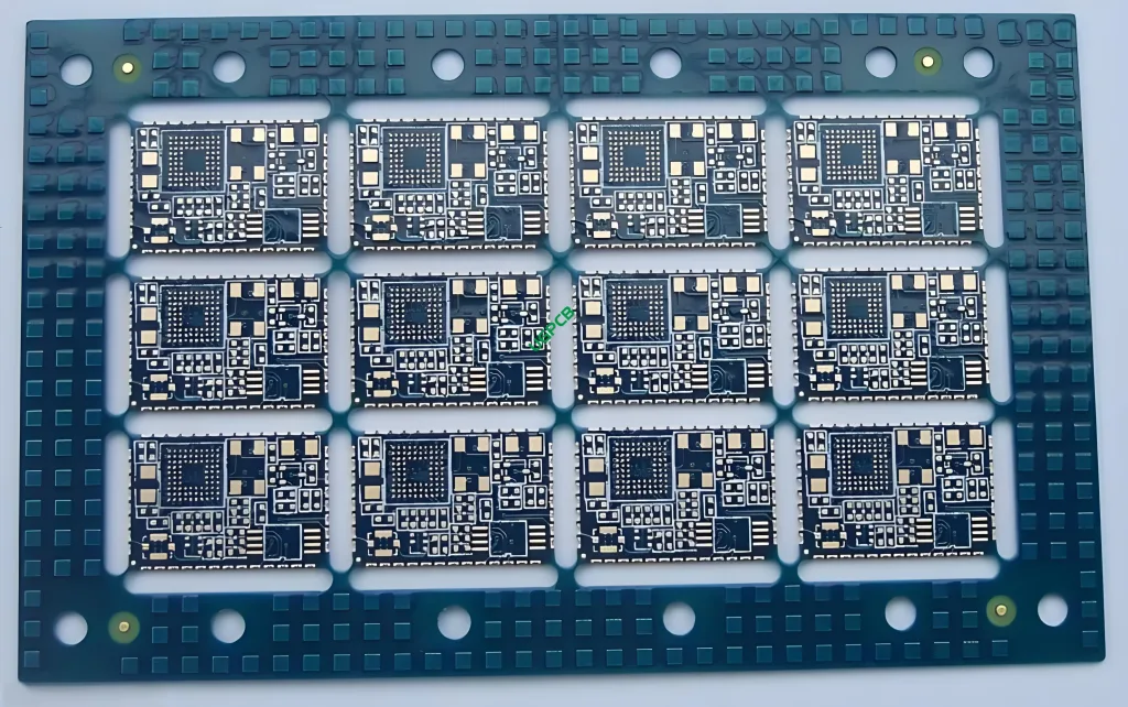
Overview of 4layers Multilayer Bluetooth PCB
The 4-layer multilayer Bluetooth ثنائي الفينيل متعدد الكلور is a specialized product designed to meet the stringent requirements of Bluetooth applications. This type of PCB offers high signal integrity, thermal stability, والموثوقية, making it an ideal choice for various Bluetooth-enabled devices.


تعريف
A 4-layer multilayer Bluetooth PCB is a لوحة الدوائر المطبوعة specifically designed to support the functions of a Bluetooth module. It consists of multiple layers of conductive and insulating مواد, providing complex electrical pathways and connections essential for the operation of the Bluetooth device. The term “4-layer” refers to the number of conductive layers, while “multilayer” indicates that it has more than two layers of conductive material.
متطلبات التصميم
When designing a 4-layer multilayer Bluetooth PCB, يجب تلبية العديد من المتطلبات الأساسية:
- جودة المواد: High-quality FR4 material is essential for durability and thermal stability.
- تكوين الطبقة: A 2-layer design is standard, allowing for efficient routing of signals and power.
- سمك النحاس: يضمن سُمك النحاس الذي يبلغ 1 أونصة التوصيل المناسب.
- المعالجة السطحية: تعمل المعالجة السطحية الذهبية المغمورة على تعزيز الاتصال ومقاومة التآكل.
- أبعاد التتبع/المساحة: الحد الأدنى لأبعاد التتبع والمساحة 4 مل (0.1مم) مطلوبة لأنماط الدوائر الدقيقة.
- ميزات خاصة: Half-hole PCB design is often incorporated for specific component placement and soldering requirements.
مبدأ العمل
The 4-layer multilayer Bluetooth PCB operates based on the principles of electrical conductivity and signal integrity. تشكل الطبقات الموصلة مسارات للإشارات الكهربائية, بينما تمنع الطبقات العازلة التفاعلات غير المرغوب فيها بين هذه الإشارات. The half-hole design allows for better signal routing and reduces crosstalk. توفر المعالجة السطحية الذهبية المغمورة اتصالاً ممتازًا وتحمي من العوامل البيئية.
التطبيقات
This type of PCB is primarily used in Bluetooth-enabled devices, which are crucial عناصر in various electronic systems such as wireless communication devices, audio equipment, and IoT (Internet of Things) devices. وتشمل هذه:
- Bluetooth speakers and headphones
- Wireless keyboards and mice
- Smart home devices
- Fitness trackers and wearables
- Industrial automation systems
تصنيف
4-layer multilayer Bluetooth PCBs can be classified based on their specific features and intended use, مثل:
- Signal Integrity Boards: For maintaining high signal quality in Bluetooth communications.
- Thermal Management Boards: To efficiently dissipate heat generated by Bluetooth components.
- لوحات التحكم: For managing and controlling various functions in Bluetooth-enabled systems.
مواد
The primary materials used in the construction of a 4-layer multilayer Bluetooth PCB include:
- المواد الأساسية: FR4, مادة من الألياف الزجاجية المقاومة للهب معروفة بخصائصها العازلة الممتازة وقوتها الميكانيكية.
- مادة موصلة: نحاس, تستخدم للآثار الموصلة.
- المعالجة السطحية: غمر الذهب, مما يعزز الاتصال ويوفر مقاومة للتآكل.
أداء
The performance of a 4-layer multilayer Bluetooth PCB is characterized by:
- سلامة الإشارة العالية: Due to the precise trace and space dimensions and half-hole design.
- Enhanced Thermal Stability: The FR4 base material helps dissipate heat more effectively.
- اتصال موثوق: يتم ضمانه عن طريق المعالجة السطحية للذهب الغمر.
- متانة: معززة بمادة FR4 الأساسية القوية.
- الكفاءة الكهربائية: تقليل فقدان الإشارة والتداخل إلى الحد الأدنى بسبب تكوين الطبقة الأمثل.
بناء
The structure of a 4-layer multilayer Bluetooth PCB consists of:
- Two Layers of Conductive Material: بالتناوب مع الطبقات العازلة.
- المعالجة السطحية بالغمر بالذهب: لتعزيز الاتصال والحماية.
- تصميم نصف فتحة: لوضع مكونات محددة ومتطلبات اللحام.
سمات
Key features of the 4-layer multilayer Bluetooth PCB include:
- Advanced Layer Configuration: 4-layer design for superior signal routing.
- دقة عالية: مع الحد الأدنى من أبعاد التتبع والمساحة 4 مل (0.1مم).
- خيارات الألوان القابلة للتخصيص: Available in black or white.
- سمك قياسي: بسمك نهائي 1.0 ملم.
عملية الإنتاج
The production process for a 4-layer multilayer Bluetooth PCB involves several steps:
- إعداد المواد: اختيار وتحضير صفائح FR4 ورقائق النحاس.
- التراص طبقة: Combining the copper and insulating layers.
- النقش: إزالة النحاس الزائد لتشكيل نمط الدائرة المطلوب.
- تصفيح: تطبيق المعالجة السطحية للذهب الغمر.
- التصفيح: دمج الطبقات تحت الحرارة والضغط.
- حفر: إنشاء ثقوب لمكونات الفتحة والمنافذ.
- تطبيق قناع اللحام: حماية الدائرة من جسور اللحام والعوامل البيئية.
- الطباعة بالشاشة الحريرية: إضافة نص ورموز لوضع المكونات وتحديد هويتها.
- ضبط الجودة: التأكد من أن PCB يلبي جميع مواصفات ومعايير التصميم.
استخدم السيناريوهات
The 4-layer multilayer Bluetooth PCB is ideal for scenarios where:
- سلامة الإشارة العالية أمر بالغ الأهمية.
- مطلوب اتصالات موثوقة ودائمة.
- Effective thermal management is necessary to maintain stable operating temperatures.
- هناك حاجة إلى معالجة سطحية متقدمة لتحسين الأداء.