


Overview of 6 Layer Golden Finger PCB
ال 6 Layer Golden Finger PCB is a high-precision, multi-layered printed circuit board designed for advanced electronic applications. This product combines multiple layers of conductive traces and insulating materials to provide exceptional performance and reliability in various electronic devices.
تعريف
أ 6 Layer Golden Finger PCB is a type of multi-layer printed circuit board (ثنائي الفينيل متعدد الكلور) that features six individual layers of conductive material, separated by insulating layers. The term “Golden Finger” refers to the specific surface treatment applied to the edges of the board, which involves immersion gold and additional gold plating on the contact fingers.
متطلبات التصميم
When designing a 6 Layer Golden Finger PCB, several key requirements must be considered:
- جودة المواد: High-quality FR4 material is essential for durability and performance.
- تكوين الطبقة: Six layers are needed to accommodate complex circuitry and signal routing.
- سمك النحاس: A standard copper thickness of 1OZ ensures adequate conductivity.
- المعالجة السطحية: Immersion gold with additional gold finger plating enhances connectivity and corrosion resistance.
- أبعاد التتبع/المساحة: A minimum trace/space of 4mil/4mil is required for precise circuit patterns.
- Special Processes: The gold finger process with a thickness of 0.1um is critical for reliable edge connections.
مبدأ العمل
ال 6 Layer Golden Finger PCB operates based on the principles of electrical conductivity and insulation. Conductive traces on different layers create pathways for electrical signals, بينما تمنع الطبقات العازلة التفاعلات غير المرغوب فيها بين هذه الإشارات. The gold finger edges facilitate easy insertion into connectors, ensuring stable and reliable connections.
التطبيقات
This type of PCB is widely used in applications that require high precision and reliability, مثل:
- High-speed digital circuits
- معدات الاتصالات السلكية واللاسلكية
- Advanced computing systems
- إلكترونيات السيارات
- Medical devices
تصنيف
6 Layer Golden Finger PCBs can be classified based on their intended use, مثل:
- لوحات معالجة الإشارات: للتعامل مع الإشارات عالية التردد في أجهزة الاتصالات.
- لوحات توزيع الطاقة: لإدارة إمدادات الطاقة في الأنظمة الإلكترونية المعقدة.
- لوحات التحكم: For controlling and managing various functions in electronic devices.
مواد
The primary materials used in the construction of a 6 Layer Golden Finger PCB include:
- المواد الأساسية: FR4, مادة من الألياف الزجاجية المقاومة للهب معروفة بخصائصها العازلة الممتازة وقوتها الميكانيكية.
- مادة موصلة: نحاس, تستخدم للآثار الموصلة.
- المعالجة السطحية: Immersion gold and additional gold plating for the gold fingers.
أداء
أداء أ 6 Layer Golden Finger PCB is characterized by:
- سلامة الإشارة العالية: نظرًا لأبعاد التتبع/المساحة الدقيقة والمواد عالية الجودة.
- اتصال موثوق: Ensured by the gold finger surface treatment.
- متانة: Enhanced by the robust FR4 base material and immersion gold finish.
- الكفاءة الكهربائية: تقليل فقدان الإشارة والتداخل إلى الحد الأدنى بسبب تكوين الطبقة الأمثل.
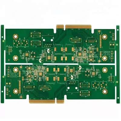
بناء
The structure of a 6 Layer Golden Finger PCB consists of:
- ست طبقات من المواد الموصلة: بالتناوب مع الطبقات العازلة.
- Gold Finger Edges: Plated with a thin layer of gold for enhanced connectivity.
- Protective Layers: Including solder mask and silkscreen for protection and identification.
سمات
Key features of the 6 Layer Golden Finger PCB include:
- المعالجة السطحية المتقدمة: Immersion gold plus gold finger for superior connection quality.
- دقة عالية: With a minimum trace/space of 4mil/4mil.
- خيارات الألوان القابلة للتخصيص: متوفر باللون الأخضر أو الأبيض.
- سمك قياسي: With a finished thickness of 1.6mm.
عملية الإنتاج
The production process for a 6 Layer Golden Finger PCB involves several steps:
- إعداد المواد: اختيار وتحضير صفائح FR4 ورقائق النحاس.
- التراص طبقة: طبقات متناوبة من النحاس والمواد العازلة.
- النقش: إزالة النحاس الزائد لتشكيل نمط الدائرة المطلوب.
- تصفيح: Applying immersion gold and additional gold finger plating.
- التصفيح: دمج الطبقات تحت الحرارة والضغط.
- حفر: إنشاء ثقوب لمكونات الفتحة والمنافذ.
- تطبيق قناع اللحام: حماية الدائرة من جسور اللحام والعوامل البيئية.
- الطباعة بالشاشة الحريرية: إضافة نص ورموز لوضع المكونات وتحديد هويتها.
- ضبط الجودة: التأكد من أن PCB يلبي جميع مواصفات ومعايير التصميم.
استخدم السيناريوهات
ال 6 Layer Golden Finger PCB is ideal for scenarios where:
- سلامة الإشارة العالية أمر بالغ الأهمية.
- مطلوب اتصالات موثوقة ودائمة.
- تتطلب قيود المساحة تصميمًا مدمجًا وفعالًا.
- هناك حاجة إلى معالجة سطحية متقدمة لتحسين الأداء.