
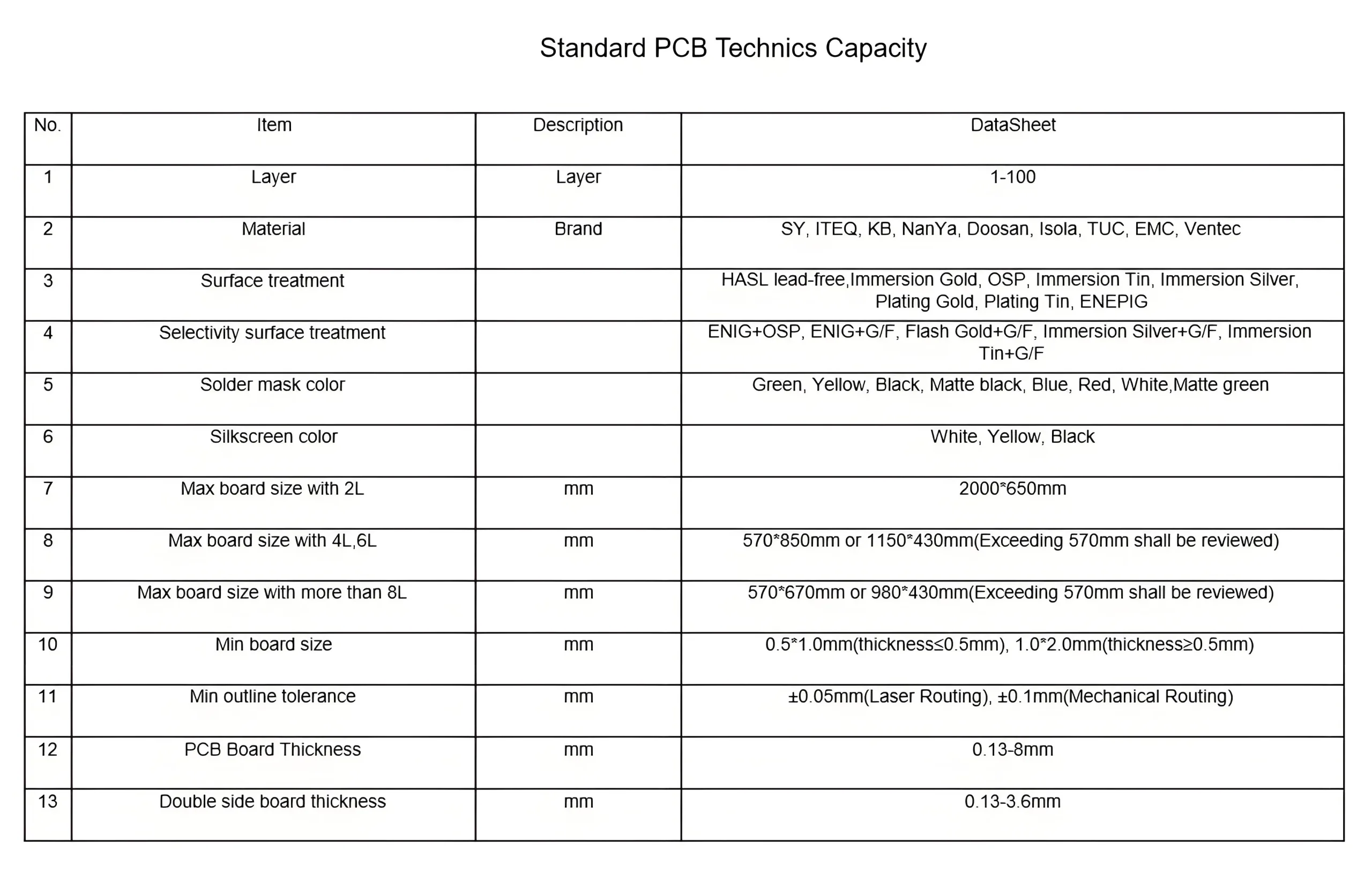

Precision Circuit Imaging & Etching Technology
UGPCB Factory demonstrates exceptional process control in circuit patterning and etching. For standard PCB production, we consistently achieve:
- Laser Direct Imaging (LDI) replacing traditional photolithography masks, enabling digital file-based exposure with ±5μm alignment accuracy
- Alkaline etching process ensuring clean line edges with ±15% line width control (industry-leading tolerance)
- Expertise in handling various copper thicknesses (1oz-6oz) with minimized side-etching
High-Precision Drilling & Hole Metallization
Our drilling capabilities cover:
- Mechanisches Bohren for 0.4mm-3.0mm boards with ±0.025mm hole size tolerance
- Laserbohrung down to 0.1mm microvias
- Hole metallization Erreichen >20μm uniform copper plating through advanced chemical deposition and electroplating
- Special processes for 8:1 Zu 10:1 aspect ratio requirements
Multilayer Lamination & Interlayer Alignment
- Up to 100-layer PCB fabrication using FR-4 Grade A materials
- Precision lamination with ±15um layer-to-layer alignment
- Temperature/pressure/time-controlled processes preventing delamination
- Options for high-Tg materials, high-speed laminates, and heavy copper up to 1000μm
Lötmaske & Surface Finish Options
- Solder mask colors: Green/Blue/Red/Black with 0.08mm minimum solder bridge
- Oberflächenbewegungen:
- Bluten (Heißluftlötes Leveling)
- ZUSTIMMEN (Elektrololes Nickel -Eintauchgold)
- Immersion Tin/Silver
- OSP (Bio -Lötlichkeitsschutz)

Comprehensive QC & Testing Systems
- AOI -Inspektion: High-resolution defect detection for line/space, Pads, shorts/opens
- Impedanzkontrolle: ±10% tolerance for high-speed/RF applications
- Elektrische Tests: Fliegende Sonde & fixture-based continuity verification
- Reliability Testing: Thermoschock, humidity resistance, flexural testing
Process Capability & Stabilität
- CPK >1.33 (4A) across critical processes, reaching 1.67 (5A) in key areas
- Line width control within ±15% (vs industry 20% Standard)
- Statistical process control (SPC) ensuring consistent production quality
PCBA One-Stop Services
- SMT Assembly: 01005 component handling with ±0.03mm placement accuracy
- Erweiterte Verpackung: BGA/Micro BGA/PoP support with X-ray inspection
- DFM Support: Impedance calculation, Stapeldesign, manufacturability analysis
Branchenanwendungen & Kontakt
Serving consumer electronics, Industrielle Steuerungen, Telekommunikation, medizinische Geräte, and automotive sectors with tailored PCB solutions. Visit our website for process capability reports and free DFM consultation.