

Einführung: Die Kriegsführung in Millimeter im DDR5-Leiterplattendesign

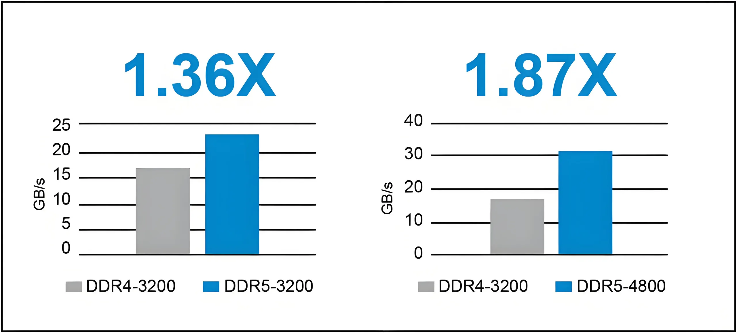
Der Sprung von DDR4 auf DDR5 markiert eine Paradigmenverschiebung: Die Signalraten steigen aus 3,200 Mt/s zu 6,400 MT/S, während die Betriebsspannungen auf 1,1 V sinken. Diese doppelte Herausforderung verändert sich Leiterplatte Routing von Simple Connectivity Engineering in Millimeter-Maßstab in Präzisionskriegsführung. Branchendaten zeigen das 80% von DDR5 -Designfehlern stammen aus Routing -Problemen, mit 90% durch Vor-Layout-Simulation vermeidbar. In diesem Artikel wird fünf kritische DDR5 -Routing -Fallstricke angelegt, unterstützt durch empirische Daten und Fallstudien, Bereitstellung umsetzbarer Lösungen für PCB -Profis.
1. DDR5 Physikalische Eigenschaften: Warum herkömmliche PCB -Designmethoden scheitern
1.1 Signalrate und Bandbreite Revolution
Für DDR5-6400, Die effektive Taktfrequenz erreicht 3,200 MHz, mit Kantenraten so schnell wie 0.5 ps (20-80% Anstiegszeit). Dies löst sich aus:
-
Verschärfte Hauteffekt: Hochfrequenzströme konzentrieren sich auf Leiterflächen, Reduzierung der effektiven Kupferdicke auf 0.66 μm at 10 GHz.
-
Dielektrikum Eskalation Eskalation: FR4 -Substrate einen Verlusttangenten aufweisen (Df) von 0.02 bei 10 GHz, Ursache >3 DB/Zoll -Signaldämpfung.
Formelvalidierung (Hauttiefe):


Bei F = 10 GHz, Δ≈0,66 μm,Traditionelle 1oz Kupfer lassen (35 μm) mit <2% Verwendung.
2. Fünf DDR5 -Routing -Minenfelder und Gegenmaßnahmen
2.1 Minenfeld 1: Timing -Fehler - die Überlebensschwelle von ± 15 PS
Auswirkungen: Eine 5-mil-Länge-Nichtübereinstimmung führt zu einer Verzögerung von ± 12 PS, kollabierende horizontale Augenbreite durch 30%.
Fallstudie: Ein GPU -Design erlitt einen Abbau von BER von 10–12 Zu 10–7 Aufgrund des 8-mil-DQ/DQS-Versatzes.
Lösungen:
-
3D Routing -Kompensation: Ersetzen Sie 90 ° -Meener durch 45 ° -Serpentine, Reduzierung der parasitären Kapazität durch 30%.
-
Dynamische Timing -Kalibrierung: Führen Sie Monte Carlo -Simulationen durch (Trittfrequenz Sigrität) Abdeckung von ± 10% Prozessvariationen.
Formel (Zeitspanne):
TMarge= TZyklus-(TCO+TFlug+TJitter)
Für DDR5-6400 (TZyklus= 0,3125 ), Systemwarnungen auslösen wenn TMarge<50 ps.
2.2 Minenfeld 2: Impedanzdiskontinuität - das 5ω -Signal Tsunami
Risiko: Über Impedanz -Fehlanpassung Ursachen >15 DB -Renditeverlust, Einstürzende vertikale Augenhöhe durch 40%.
Daten: Jeweils unoptimiert durch Adds 0.2 DB -Einfügungsverlust bei 5 GHz.
Lösungen:
-
Über Revolution: Implementieren Sie Laserblind-Vias (≤ 4mil) mit Antipad -Kompensation, Einschränkungsimpedanzschwankung auf ± 3 Ω.
-
PAD -Optimierung: Verwenden Sie elliptische Pads (1.5:1 Seitenverhältnis) kapazitive Effekte zu reduzieren durch 20%.
Formel (Über Impedanzmodell):
Zvia ~ 87ϵr · ln(5.98H/(0.8D1+D2))
Wo : dielektrische Dicke, D1: über Durchmesser, : Paddurchmesser.
2.3 Minenfeld 3: Verzögerung der Verringerung-der 0,1ps/mm-Schmetterlingseffekt
Fasergewebeeffekt: Dielektrizitätskonstante Variation (Δϵr = 0,3) aus Glasfaser -Periodizität verursacht 0.6 PS/Zoll Verzögerungsversatz.
Lösungen:
-
Z-Achsenausrichtung: Routenbyte-Gruppen-Signale bei ± 45 ° Winkel, um die dielektrische Anisotropie abzubrechen.
-
Vergleichskompensation: Vorlast -Substrat DK/DF -Daten in EDA -Tools zur automatischen Verzögerungskorrektur.
2.4 Minenfeld 4: Power Ripple - die 1MV -Kernkettenreaktion
Empfindlichkeit: 50MV Ripple bei 1,1 V erhöht den Fahrer Jitter nach 20%.
Simulation: Die PDN -Zielimpedanz muss ≤ 2 Mω@100 MHz - 5x strenger sein als herkömmliche Designs.
Lösungen:
-
3D Kondensatormatrix: Einsetzen 0,1 μf (0402) + 10nf (0201) Kondensatoren in der Nähe von ICs, Abdeckung 10 KHz - 2 GHz.
-
Mikro-Koper-Säulen: Einbetten Sie 200 & mgr; m-Säulen unter BGAs ein, Schneiden von Schleifeninduktivität durch 30%.
2.5 Minenfeld 5: Störung des Rückwegpfads - die unsichtbare EMI -Bombe
EMI -Risiko: Zerbrochene Referenzebenen erzeugen Common-Mode-Rauschen, überschreiten EMI -Grenzen durch 10 db.
Lösungen:
-
Bodennähte: Platzieren Sie gemahlene Vias (≤ 0,1o) jeder 100 mil zwischen Signalschichten.
-
Überbrückung von Split-Ebenen: Verwenden Sie begrabene Kondensatoren (z.B., AVX 0402B) Für 10 NF -Kopplung über Power Splits.
3. DDR5 Design Golden Regeln: Formeln und Toolchains
3.1 Über Stubbeschränkung:Für DDR5-6400 (F = 3,2 GHz) auf fr4: StummelMax≤ 13,7 mm.


3.2 Differentialpaartoleranz:
Mit TUi= 0,3125 ns Und vP= 6 Zoll/: ΔL ≤ 1,9 mil.


3.3 PDN -Impedanzziel:
Für 50mV Ripple und 10A Transientenstrom: ZZiel≤ 5 MΩ.


4. PCB -Konstruktionsprozess neugineering: Von Versuch und Irrtum bis hin zu simulationsgetriebenen
4.1 Topologieplanung:
-
Modell VIAS in HFSS; Optimieren Sie die Antipad -Dimensionen.
-
Extrahieren Sie die Stackup -Impedanz über Siwave; Bauen Sie S-Parameter-Bibliotheken auf.
4.2 Routing -Ausführung:
-
Aktivieren Sie Echtzeit-Impedanzkontrollen in Allegro; Verstöße gegen die Autoflagge.
-
Durchsetzen.

4.3 Validierung:
-
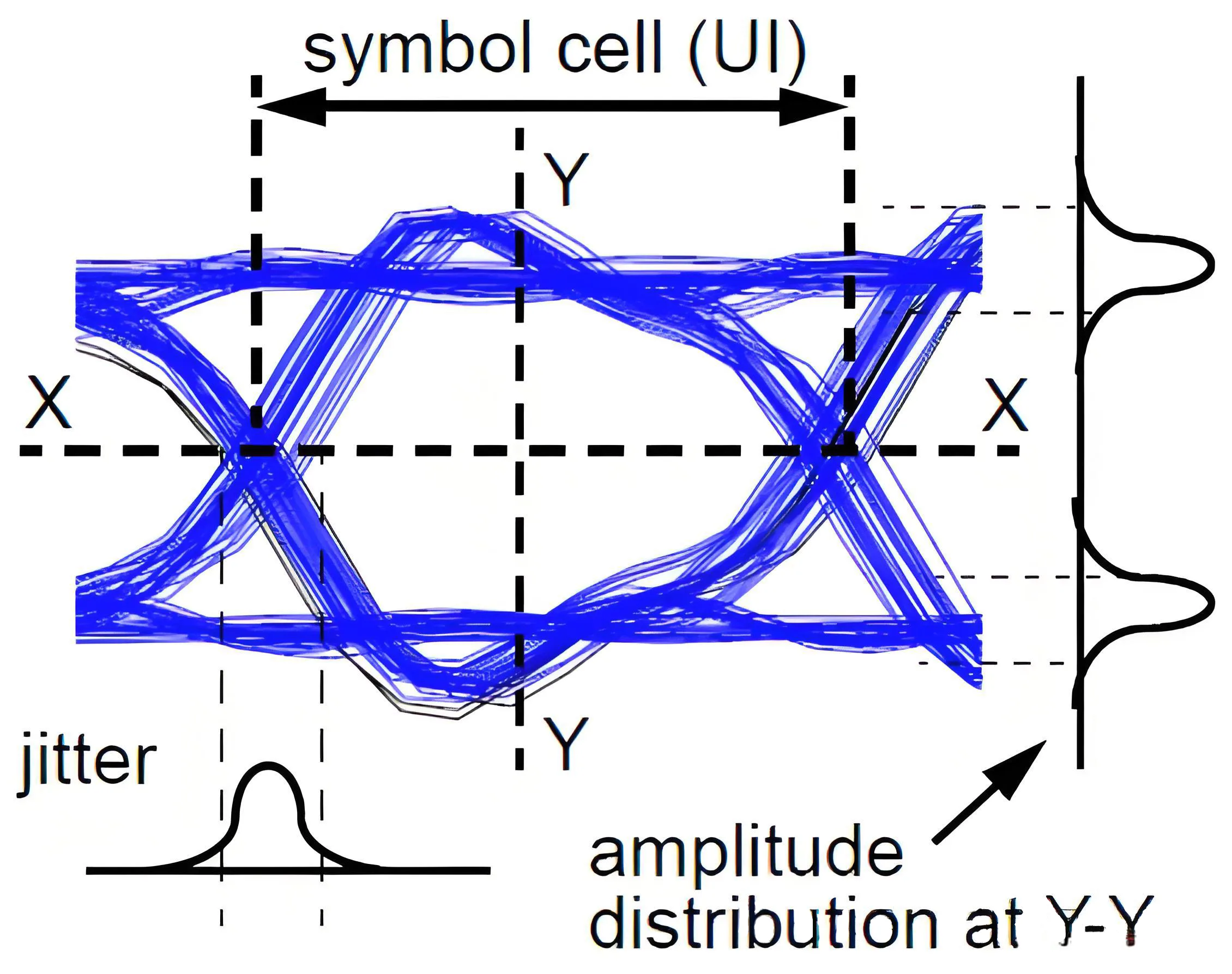
Führen Sie Augendiagrammtests durch (Keysight -Anzeigen) mit ≥70 mV Augenhöhe.
-
Messen Sie TDR -Kurven; Grenzeimpedanzschwankungen auf ± 5% begrenzen.
Abschluss: The “Three-Body” Law of DDR5 Design
Unter GHz-Geschwindigkeit, Hügel -Nuic, und Mikron-Toleranzbeschränkungen, DDR5 PCB design enters a “quantum mechanics” era. Sieg in der Signalintegrität Kriegsführung fordert die Konvergenz der Materialwissenschaft (Low-DK-Substrate), fortgeschrittene Prozesse (MSAP), und Simulation Meisterschaft.