
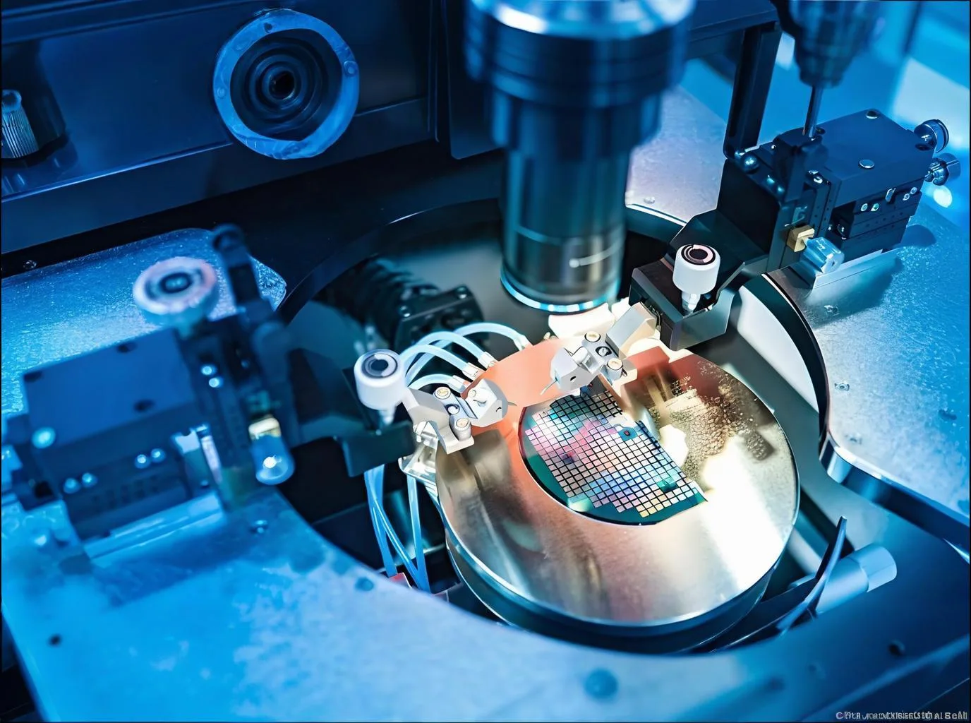
Jeder mikroskopische Fortschritt in der Verpackungstechnologie umgestaltet die physikalischen Grenzen der Elektronik.

In der letzten Woche Entwicklung der Chipverpackung: Vom Eintauchen zu X2SON - wie Miniaturisierung die Elektronik umgestaltet hat, Wir haben die Ära der Durchlögelverpackung untersucht (TAUCHEN) und wie Oberflächenmontagegeräte (SOP, Beobachtung, SOHN) Initiierte Geräteminiaturisierung. Während diese Technologien moderne Verpackungsstiftungen legten, Die Miniaturisierungsrevolution fährt fort. Heute, Wir untersuchen Pakete mit höherer Dichte-von Quad-Flat bis Wafer-Level-CSP-und deren Auswirkungen auf PCB-Design Grenzen.
Quad-Flat-Pakete: Die Raumdichte Balance
Quad-Flat-Pakete (MFR, PLCC/QFJ, QFN) Stellen Sie eine kritische Entwicklung in Richtung höherer E/O -Dichte durch, indem Sie alle vier Paketkanten verwenden.
MFR: Die Pionier der Möwenflügeldichte
MFR (Quad -Flat -Paket) features iconic “gull-wing” (L-förmig) Leads, die sich von allen Seiten erstrecken. Es ist Pin -Tonhöhe (0.4mm/0,5 mm/0,65 mm) diktiert PCB -Routing Dichte und Löten Präzision.
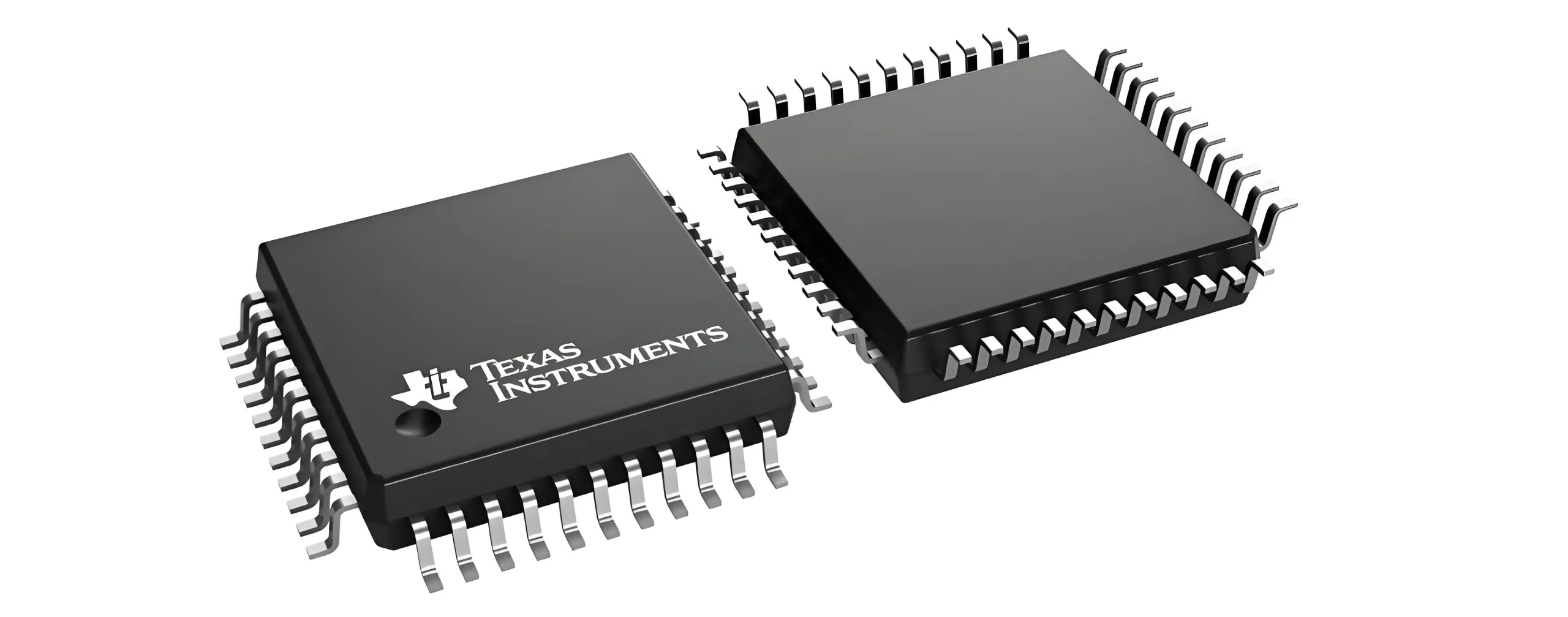

QFP -Varianten:
-
Größe/Dicke: Lqfp (Niedrig profiliert), Tqfp (Dünn), VQFP (Sehr dünn)
-
Material: PQFP (Plastik), MQFP (Metall)
-
Thermisch verstärkt: HQFP, Hlqfp, Htqfp, Hvqfp
-
Schutz: BQFP (Stoßfänger - Corner -Pads verhindern gebogene Leitungen)
Das thermische Management ist kritisch. Die Formel zur Thermalwiderstandsübergangsübergang zu Ammie θja = (Tj - ta)/P (Wo Tj= Junction -Temperatur, Gesichtsansicht= Umgebungstemperatur, P= Macht) regiert das Design der Wärmeabteilung.
PLCC/QFJ: Stabilität durch J-Leads
PLCC (Plastik -Blei -Chipträger) oder qfj (Quad Flat J-beladen) Verwendet J-förmige Abwärtskörper nach unten für die mechanische Stabilität gegen Vibration/Wärmespannung.


Standardisierungsvorteil: Die hohe Kompatibilität von PLCC/QFJ mit universellen Teststecks rationalisiert die Produktionstests. Obwohl QFJ technisch präzise ist, “PLCC” remains industry-preferred.
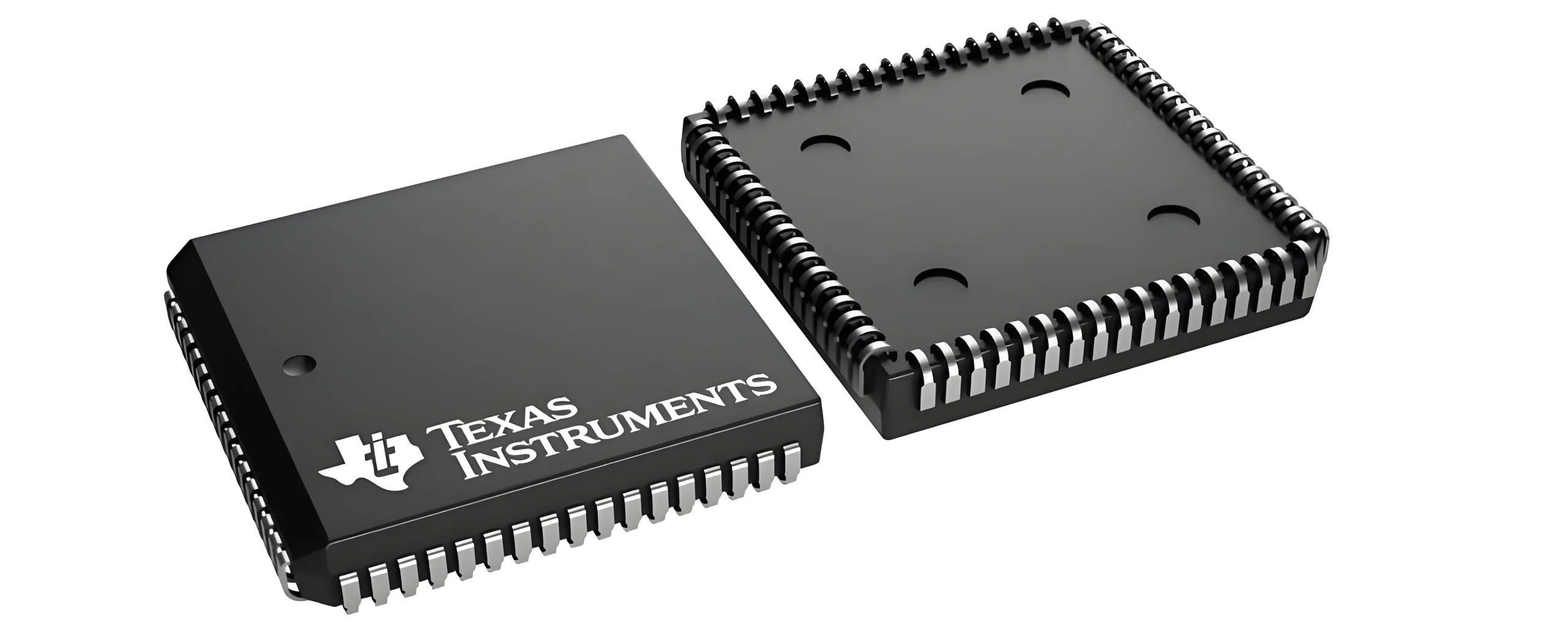
QFN: Durchbruch ohne Leadless Miniaturisation
QFN (Quad Flat No-Lead) eliminiert externe Leads, Verbindung über:
-
Exponiertes Pad (EP): Direkter thermischer Weg zu Leiterplatte Kupfer
-
Benutzbare Flanken: Lötkads mit Seitenwand
Schlüsselvorteile:
-
Ultra-Kompakt: 40% kleiner als QFP
-
Elektrische Überlegenheit: Kürzere Wege verringern die parasitäre Induktivität (L ≈ μ · L/W.)
-
Wärmeeffizienz: Niedrigere θja vs. Gleiche QFP
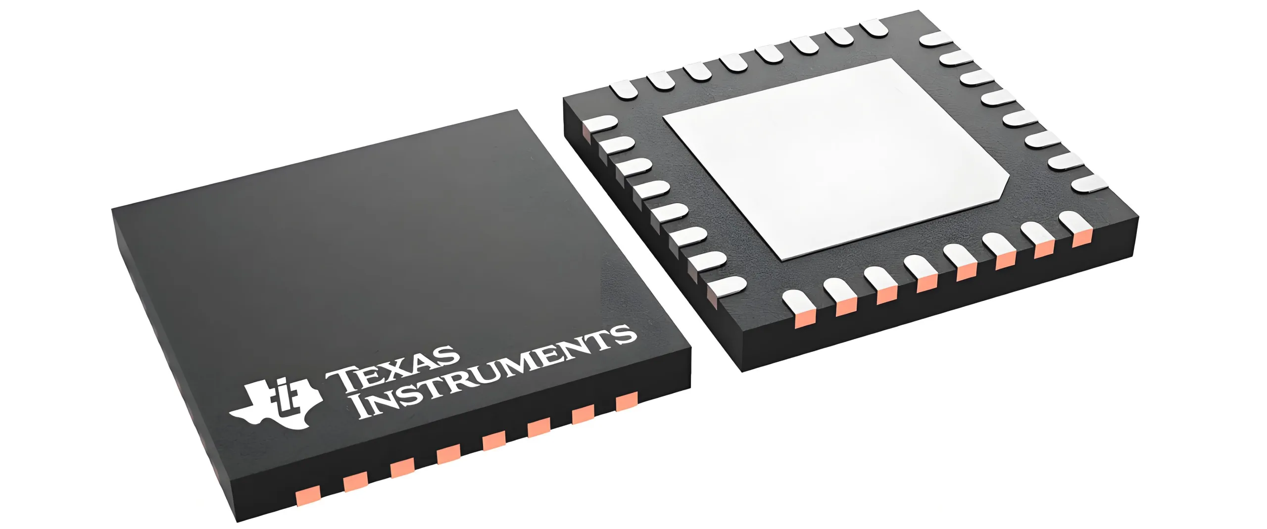

Dickeentwicklung: Lqfn → uqfn → vqfn → wqfn → x1qfn → x2qfn. LCC (LPCC/LCCC) ist seine baderlose Keramik/Plastikvariante.
Array -Pakete: Dichtegrenzen revolutionieren
Wenn Quad-Flat E/A-Grenzen erreicht, Array -Pakete (LGA, BGA) Aktivieren Sie die 2D -Verbindungsdichte.
LGA: Präzise elastische Verbindung
LGA (Landgitterarray) Verwendet präzise ausgerichtete Metallkontakte (z.B., LGA775: 775 Kontakte) Paarung mit Stecknadeln.
Kernwert:
-
Saugbarkeit: CPU -Upgrades/Wartung
-
Niedrige Induktivität: Kurze Signalwege
-
Hohe Zuverlässigkeit: Ideal für CPUs (Intel/AMD)
Einschränkung: Hohe Sockelkosten/Größe bevorzugt BGA in kompakten Geräten. Notiz: LGAs können direkt-smt verkauft werden.
BGA: Die Dominanz der Lötkugel
BGA (Kugelgitter-Array) verbindet sich über eine Lötkugelmatrix. Ball Tonhöhe (0.3–1,0 mm; <0.2MM für FBGA) ist kritisch.
Transformative Vorteile:
-
Hohe Dichte: >1,000 Ich/wir (vs. QFPs ~ 300)
-
Raumsparung: 30%+ Bereichsreduzierung vs. MFR
-
Elektrisch/thermisch: Niedrige Signalverzögerung; Kugeln leiten Wärme
-
Selbstausrichtung: Oberflächenspannung hilft
BGA -Familie:
-
Material: PBGA (Plastik), CBGA/CABGA (Keramik)
-
Größe/Tonhöhe: nFBGA/FBGA (Feinkopie), Tinybga, DSBGA/WCSP (Die Größe sterben), LFBGA/VFBGA (Dünn)
-
Integration:
-
FCBGA (Flip-Chip): Direkte Anschluss an Substrate über Mikrobumps
-
Pop (Paket-on-Package): Vertikales Stapeln (z.B., Logik + Erinnerung)
-
PG-WF2BGA: Fan-Out-Wafer-Level-Verpackung
-

Herausforderungen: Röntgeninspektion (Axi), Komplexe Nacharbeit, CTE-Matching PCB -Materialien.
Array -Paketvergleich
| Besonderheit | PGA (Pin -Raster -Array) | LGA (Landgitterarray) | BGA (Kugelgitter-Array) |
|---|---|---|---|
| Verbindung | Starre Stifte | Planare Kontakte | Lötkugeln |
| Schlüsselstärke | Sockelzuverlässigkeit | Dichte + stockbar | Maximale Dichte/min -Größe |
| Signalverzögerung | Höchste | Medium | Niedrigste |
| Anwendungen | Legacy CPUs/Industrial | Desktop/Server -CPUs | Mobile/GPU/SOC |
| PCB -Speicherplatz | Groß | Medium | Kompakt |
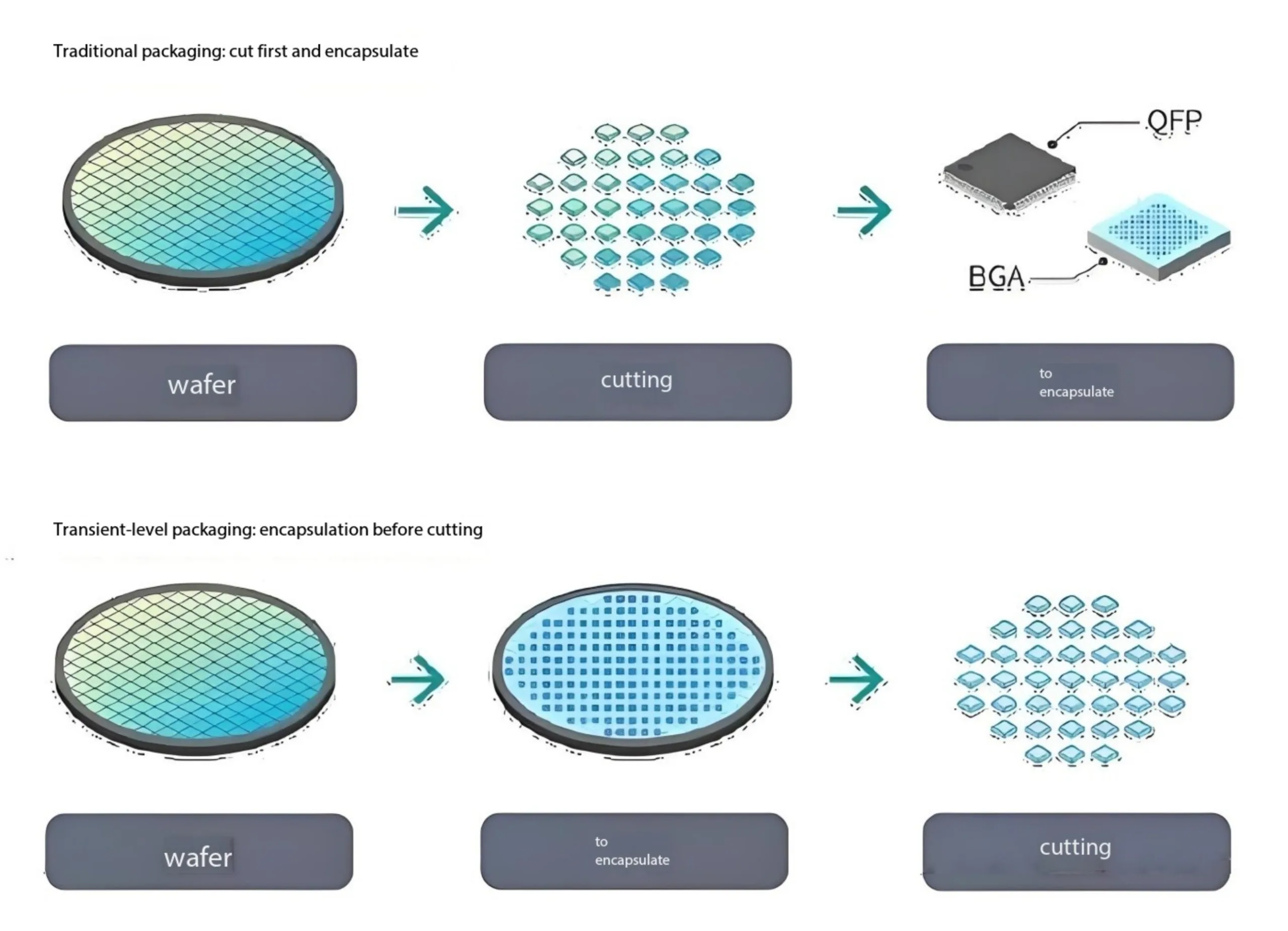
Chip-Scale & Pakete auf Waferebene: Annäherung an die physischen Grenzen
CSP: Größengrenzen neu definieren
CSP (Chip -Skala -Paket) Schlüsselmetrik: Paketgröße ≤ 1,2 × Würfelgröße (vs. 2–5 × für traditionelle). Im Wesentlichen miniaturisierte BGA (FBGA/VFBGA) mit feinerer Tonhöhe (0.2–0,5 mm).
Wert: Ultimative Miniaturisierung für Wearables/Sensoren.
Ulc: Die Revolution auf Waferebene
Die WLCSP/Wafer-Level-Verpackung führt alle Schritte aus (Rdl, Balling) auf dem Wafer vor dem Würfeln.
Störende Vorteile:
-
Minimale Größe: ≈ Die Dimensionen
-
Kostensenkung: 30-50% billiger (Keine Substrate/Formteile)
-
Spitzenleistung: Kürzeste Verbindungen, niedrigste Parasitik

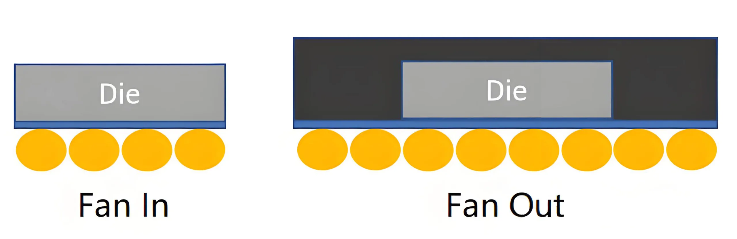
WLCSP -Typen:
-
Fan-in WLCSP:
-
Bälle in der Fläche
-
Paketgröße = Stanzgröße
-
Niedrigpreis für Sensoren/PMICs
-
-
Fan-Out WLCSP (z.B., TSMC Info, Samsung fo-plp):
-
Bälle erstrecken sich über die Sterbchen hinaus
-
Paketgröße > Größe
-
Höhere E/O -Dichte, Multi-Chip-Integration
-
Für Premium -SoCs/RF -Module
-

Visuelle ID: Unkapseliges Silizium (vs. Harzmolded DFN).
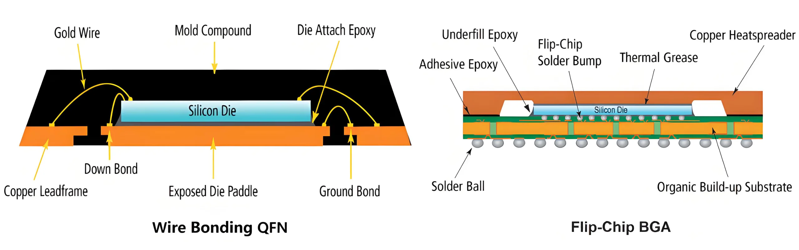
Verpackungsmorphologie & Bindungstechniken
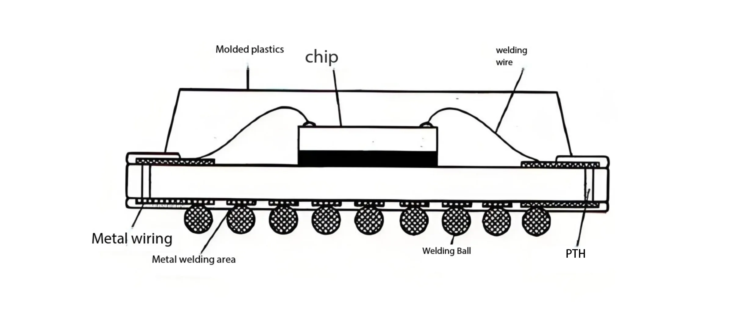
Externes Paketformular (QFP/BGA/WLCSP) und interne Bindung sind intrinsisch miteinander verbunden:
-
Kabelbindung:
-
Reifen, niedrige Kosten
-
Dominiert QFP/QFN/Mittelklasse-BGAs
-
Haben/mit Drähten; moderates i/o
-
-
Flip-Chip:
-
Die Sterbe befestigen den Face Down über Mikrobumps
-
Kürzeste Verbindungen, niedrigste Induktivität
-
Essentiell für FCBGA/WLCSP/Hochleistungs-CSP
-

Abschluss & Zukünftige Grenzen
Von QFP zu LGA/BGA und schließlich CSP/WLCSP, Die Evolution der Chipverpackung ist a Raumkomprimierung Chronik, Leistungssteigerungen, und Kostenoptimierung. Jede Miniaturisierungspuad -Reshapes -PCB, Mehrschicht HDI, und fortschrittliche Materialien.
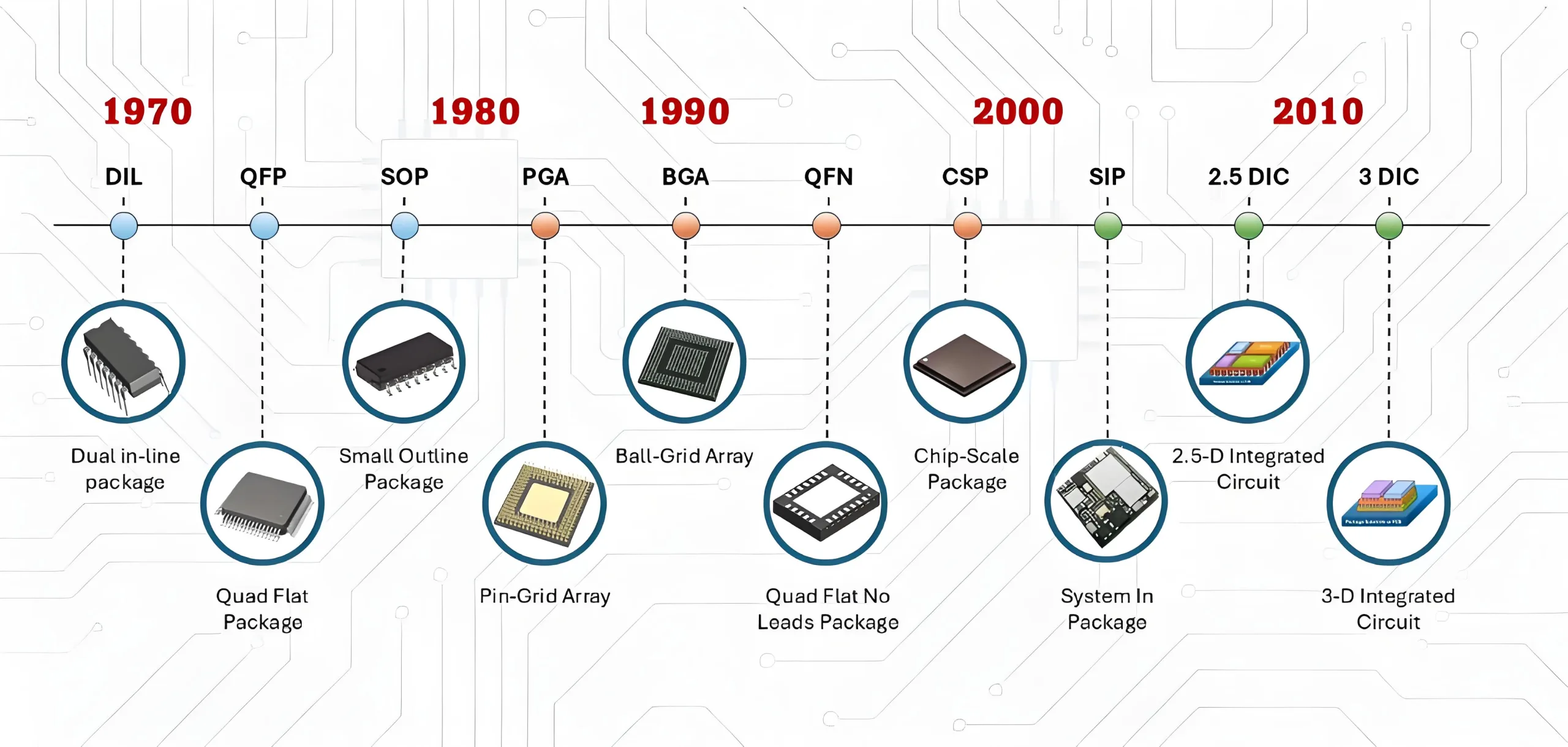

Nächste Grenze: Technologien wie TSV (Durch-Silizium über), Schluck (System-in-Package), und 2,5D/3D IC jetzt aktivieren 3D -heterogene Integration, Wenn Sie das PCB -Design in neue Dimensionen drücken - in unserem nächsten Artikel untersucht zu werden.
Wenn eine Milliarde Transistoren in ein Paket in Sandgröße in Sandalgröße passen, Elektrotechnik Schlachten im molekularen Maßstab.