

In SMT-Bestückung, Ein Fehler im Mikrometerbereich kann die Qualität beeinträchtigen. Für Leiterplatte Designer und Leiterplatte Produktionsleiter, hartnäckige Lötkügelchen auf Chip-Komponenten-Pads (wie Widerstände und MLCC-Kondensatoren) sind ein häufiges Problem. Diese Mängel beeinträchtigen die Ästhetik und können bei anspruchsvollen Anwendungen zu Kurzschlüssen führen, die Produktzuverlässigkeit gefährden. Dieser Leitfaden analysiert die fünf Hauptursachen für Lotkugeln und bietet eine Systematik, IPC-basierendes Lösungsgerüst zur Verbesserung der Lötausbeute.

Der Kernmechanismus: Paste Squeeze und Failed Containment
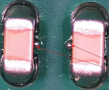
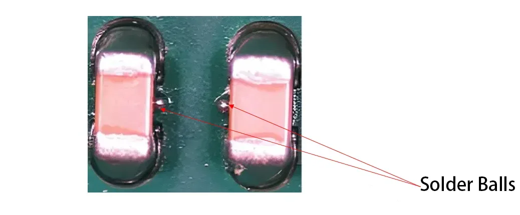
Solder balls “escape” rather than “form.” During reflow, Aufgrund der Oberflächenspannung gelingt es der geschmolzenen Lotpaste nicht, in der Hauptverbindung zusammenzuwachsen, an den Belagkanten ablösen und zusammenballen. Pro IPC-A-610, Eine Lötkugel ist ein Defekt, wenn ihr Durchmesser 0,13 mm überschreitet oder wenn die Gefahr besteht, dass Leiter überbrückt werden.
Die Hauptursache ist, dass beim Drucken oder Bestücken Lötpaste auf die Lötstoppmaske gedrückt wird. Der nicht benetzbare Lötstopplack verhindert, dass sich die Paste wieder mit der Hauptverbindung verbindet, Bildung unabhängiger Kugeln.
Grundursache 1: PCB Design “Topography”
PCB-Design ist die erste Verteidigung. Schlechtes Pad- und Lötmaskendesign schafft Fluchtwege.
1. Lötstopplackdämme: Zum Behalten oder Entfernen?
Herkömmliche Lötstopplackdämme zwischen benachbarten Chip-Pads verhindern eine Brückenbildung, erzeugen jedoch Pasteneinfanggräben. Durch die Entfernung des Damms wird dieses Gelände beseitigt, Dadurch kann sich die Paste sauber auf dem Pad ablagern und sorgt so für eine einheitliche Kontrolle der Oberflächenspannung während des Reflow-Lötens.
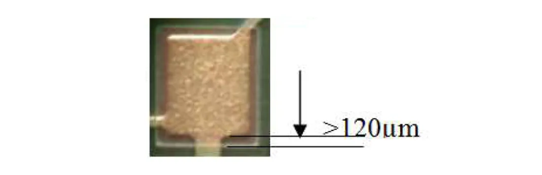
2. Öffnung der Lötmaske (SMD): Stellen Sie sicher, dass ausreichend Puffer vorhanden ist
Das SMD muss größer sein als das Kupferpad. IPC-7351 empfiehlt mindestens 75 µm (3Mil) einseitiger Spalt für Chip-Komponenten, mit 120µm (5Mil) als Best Practice. Dieser Puffer gleicht geringfügige Fehlausrichtungen der Lötstoppmaske aus, Stellen Sie sicher, dass die Paste nur das benetzbare Kupfer berührt.

3. Fertigungstoleranzen verwalten
Arbeiten Sie mit Ihrem zusammen PCB-Lieferant. Geben Sie strenge Toleranzen für die Ausrichtung der Lötmaske an (typischerweise ≤50µm) und wählen Sie einen Lieferanten, der in der Lage ist, diese innerhalb der Pufferzone Ihres Designs zu erfüllen.
Grundursache 2: Stencil Design “Dosage Control”
Der Schablone bestimmt Volumen und Form der Paste.
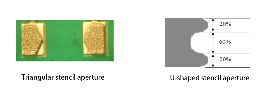
1. Volumenreduzierung & Gestaltung: U-förmige/dreieckige Öffnungen
Für 0402 und größere Komponenten, Pastenvolumen reduzieren. Erweiterte Designs verwenden U-förmige oder dreieckige Öffnungen statt Quadrate. Dadurch wird das Volumen in der Mitte reduziert, während die Paste zu den Pad-Enden geleitet wird, Bereitstellung von ausreichend Lot bei gleichzeitiger Minimierung des Herausquetschens. Dadurch kann das Pastenvolumen um reduziert werden 15-20%.
2. Blendenverhältnis optimieren
Die Breite der Schablonenöffnung beträgt typischerweise 80-90% der Padbreite. Stellen Sie sicher, dass eine Flächenverhältnis > 0.66 für saubere Ausgabe und präzise Lautstärkeregelung.

Grundursache 3: Pursuing “Zero Gap” in Paste Printing
Beim Drucken wird die anfängliche Platzierung der Paste festgelegt.
1. Erreichen Sie echten lückenlosen Kontakt
Jede Lücke zwischen Schablone und Leiterplatte führt zum Ausbluten der Paste unter dem Druck des Rakels. Stellen Sie eine flache Stützplattform und eine optimale Pin-Platzierung für eine gleichmäßige Leiterplattenunterstützung sicher. Maschinenparallelität regelmäßig kalibrieren.
2. Achten Sie auf Reinigung und Ausrichtung
Durch angetrocknete Paste auf der Schablonenunterseite entstehen Lücken. Führen Sie häufiges Wischen von der Unterseite durch (z.B., jeder 5-10 Platinen für Fine-Pitch-Komponenten). Nutzen Sie die hochpräzise Bildausrichtung für eine perfekte Ausrichtung zwischen Schablone und Pad.
Grundursache 4: “Gentle” Component Placement
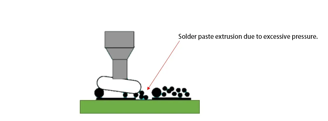
Durch die Platzierung kann die Paste zerdrückt werden.
Eine zu hohe Z-Kraft oder eine geringe Platzierungshöhe führen dazu, dass die Paste herausgedrückt wird. Stellen Sie die ein Höhe der Komponentenplatzierung Zu 1/2 Zu 2/3 der Post-Print-Pastenhöhe. This allows the part to “kiss” the paste without impact.

Grundursache 5: Reflow “Thermodynamic” Control
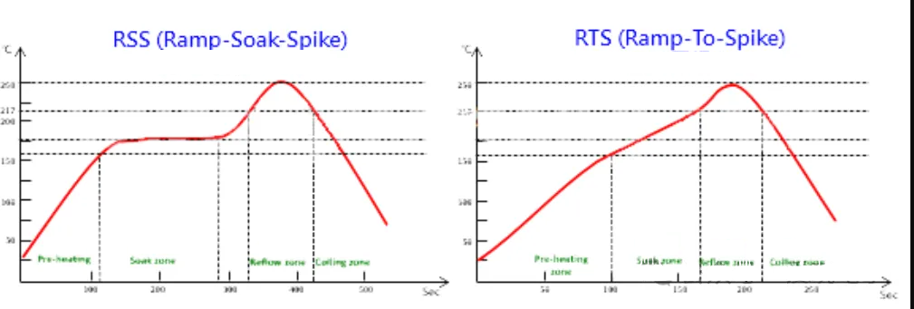
Das Reflow-Profil, vor allem vorheizen, ist kritisch.
1. Avoid Extended Preheat and “Hot Slump”
Long soak zones can cause “hot slump”: Durch vorzeitige Flussmittelverdunstung/Viskositätsabfall sinkt die Paste ab und verteilt sich auf der Lötstoppmaske, bevor sie schmilzt, was zur Kugelbildung führt.
2. Verwenden Sie ein Ramp-to-Peak- oder lineares Profil
Verkürzen oder beseitigen Sie das Einweichplateau. Verwenden Sie einen kontrollierten linearen Anstieg von Umgebungstemperatur zu Spitzenwert, mit einer Vorheizrate von 1,0–2,0 °C/Sek. Dies verkürzt die Verweilzeit bei niedrigen Temperaturen, begrenzt den Einbruch, und ermöglicht synchrones Schmelzen für eine effektive Oberflächenspannungsziehung.
Datenpunkt: Pro IPC/JEDEC J-STD-020, für SAC305-Lötmittel, Ziel 60-90 Sekunden über der Flüssigkeit (VON) und ein Spitzenwert von 235–245 °C. Optimieren Sie die Vorheizneigung innerhalb dieser Einschränkungen.

Abschluss: Ein systemischer Optimierungsansatz
Das Lösen der Lotkugeln von Chipkomponenten erfordert a Systemtechnik Ansatz quer PCB-Design, Schablonenherstellung, SMT-Druck, Komponentenplatzierung, und Reflow -Löten.
Checkliste zur Reduzierung von Lotkugeln:
-
PCB-Design: Werden Lötstopplackdämme entfernt?? Sind SMD-Öffnungen ≥120µm?
-
Schablonendesign: Werden U-förmige/dreieckige Öffnungen verwendet?? Stimmt das Öffnungsverhältnis??
-
Druckprozess: Wird die Schablone häufig gereinigt?? Ist die Ausrichtungsgenauigkeit hoch??
-
Vermittlungsprogramm: Ist die Platzierungshöhe auf eingestellt? 1/2 - - 2/3 der Pastenhöhe?
-
Reflow -Profil: Können Sie eine lineare Rampe mit kontrollierter Vorheizrate implementieren??
Für hochzuverlässige Produkte, einen Fachmann beauftragen PCBA-Hersteller für Design für die Herstellung (DFM) Überprüfen Sie frühzeitig. Ein erfahrener EMS-Partner kann Risiken erkennen und bewährte Lösungen anbieten. Durch kollaboratives Design und Prozesskontrolle, Die Anzahl der Lotkugeln kann innerhalb der IPC-Akzeptanzgrenzen minimiert werden, Erzielung einer höheren Ausbeute beim ersten Durchgang und einer überlegenen Leiterplattenzuverlässigkeit.