
In der modernen Elektronikherstellung, Prozessmängel in Leiterplatte (Montage von Leiterplatten) kann zu einer verringerten Produktzuverlässigkeit führen, erhöhte Produktionskosten, und sogar Projektfehler. Statistiken zeigen, dass PCBA-Prozessdefekte mehr als ausmachen 30% von Frühausfällen elektronischer Produkte, wobei Lötstellenprobleme und Beschichtungsfehler die Hauptfehlerarten sind. Dieser umfassende Leitfaden analysiert systematisch zehn typische Prozessfehler in PCBA-Herstellung– von der Plattierungsrauheit und Kupferpartikeln bis hin zu BGA-Lötstellenrissen – und bietet IPC-Standard-konform, praxiserprobte Lösungen, die Ingenieuren dabei helfen, die Produktqualität und -zuverlässigkeit zu verbessern.

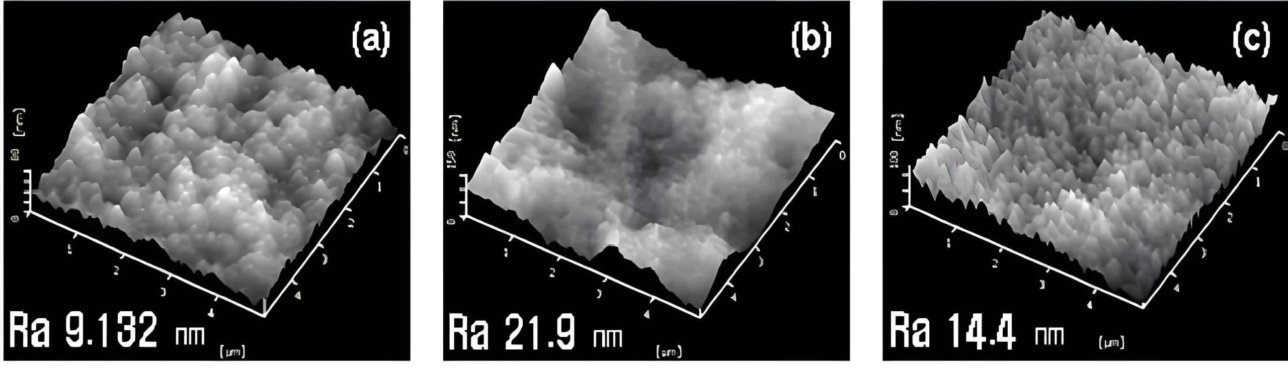
1. Rauheit der Beschichtung: Der unsichtbare Killer der Oberflächengleichmäßigkeit
Die Rauheit der Beschichtung ist ein häufiger Fehler Leiterplattenherstellung, gekennzeichnet durch raue Kanten oder eine körnige Oberflächenstruktur. Kantenrauheit ist häufig auf übermäßigen Strom zurückzuführen, der zu einer ungleichmäßigen Beschichtung führt, während die Rauheit der gesamten Platine häufig auf einen unzureichenden Glanzmittelgehalt in Umgebungen mit niedrigen Temperaturen oder auf eine unzureichende Vorbereitung der Nachbearbeitungsplatine zurückzuführen ist.

Lösungen:
- Passen Sie die Beschichtungsparameter an: Reduzieren Sie die Stromdichte und kalibrieren Sie Amperemeter für einen stabilen Ausgang.
- Optimieren Sie den Einsatz von Additiven: Ergänzen Sie bei niedrigen Temperaturen Aufheller, um die Gleichmäßigkeit zu verbessern.
- Vorbehandlung verstärken: Rework-Platinen gründlich reinigen, um Verunreinigungen und Oxide zu entfernen.
Gemäß IPC-Standards, hochwertige Leiterplatten muss eine Kupferdickentoleranz von ≤5 % einhalten. Die Rauheit der Beschichtung liegt häufig darüber 10% Abweichung, wirkt sich entscheidend auf die Strombelastbarkeit aus.
2. Kupferpartikel auf Leiterplattenoberflächen: Mikrokontamination in der Prozesskette
Kupferpartikel manifestieren sich als anhaftende Kupferkörner auf der Plattenoberfläche, stammen aus Quellen wie hoher Härte in alkalischem Entfettungswasser, Ausfälle des Filtersystems, verunreinigte Aktivatoren bei der Verkupferung, oder unvollständige Reinigung während der Bildübertragung.
Minderungsstrategien:
- Verbessern Sie die Filterwartung: Ersetzen Sie die Filterelemente regelmäßig, um die Sauberkeit des Bades zu gewährleisten.
- Waschabläufe optimieren: Sorgen Sie für eine gründliche Spülung nach der Bildübertragung und minimieren Sie die Lagerzeit des Panels.
- Überwachen Sie die Badparameter: Kontrollieren Sie den Kupfergehalt und den Säuregehalt, Verwendung von phosphorisierten Kupferanoden mit gleichmäßiger Verteilung.
3. Lochfraß in der Beschichtung: Der stille Killer der fleckigen Beschichtung
Plattierungslöcher erscheinen als fleckige Hohlräume auf Leiterplattenoberflächen, verursacht durch verunreinigte Kleiderbügel aufgrund unzureichender Reinigung, nicht gewartete bildgebende Ausrüstung, oder hartes Wasser in Vorbeschichtungsprozessen.
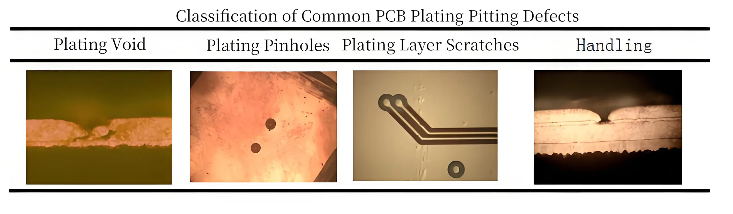

Lösungen:
- Implementieren Sie Tiefenreinigungsprotokolle für verkupferte Kleiderbügel.
- Planen Sie regelmäßige Wartungsarbeiten für die bildgebenden Geräte ein, um eine saubere Entwicklung sicherzustellen.
- Verwenden Sie zum Vorplattieren entionisiertes Wasser und ersetzen Sie abgenutzte Kleiderbügelbeschichtungen umgehend.
4. Oberflächenweißling und Farbinkonsistenz: Sehfehler mit mehreren Ursachen
Oberflächenweißung und Farbschwankungen entstehen durch ungleichmäßige Luftbewegung, die zu Schwankungen der Beschichtungsdicke führt, undichte Filterpumpen, verunreinigte Baumwollfilter, unausgeglichene Mikroätzmittelkonzentrationen, schlechte Wasserqualität, oder fehlerhafte Anodenanschlüsse.
Verbesserungsmaßnahmen:
- Passen Sie die Positionen der Luftdüsen an, um eine gleichmäßige Bewegung zu gewährleisten.
- Ersetzen Sie qualifizierte Filtermedien, um organische Verunreinigungen zu kontrollieren.
- Optimieren Sie Mikroätzprozesse, Verbesserung der Wasserqualität, und überprüfen Sie die Anodenverbindungen.
Figur: Die Qualitätsprüfung von PCBA-Platinen unter einem Mikroskop mit hoher Vergrößerung zeigt die Rauheit der Beschichtung und Kupferpartikel – kritische Mängel, die Aufmerksamkeit erfordern.
5. Defekte beim Löten von Durchgangslochgeräten: Zuverlässigkeitsherausforderungen
THD-Lötfehler, wie zum Beispiel 8.7% Fehllöten in industriellen Steuerplatinen, ergeben sich aus drei Kernthemen:
- Materielle Faktoren: Schwankungen in der Glasfaserwebdichte führen zu einer ungleichmäßigen Wärmeverteilung.
- Prozessfaktoren: Unzureichende Temperaturprofilierung während der manuellen Nacharbeit.
- Designfaktoren: Seitenverhältnisse (Lochdurchmesser/Stiftdurchmesser) unten IPCs 1.5 Empfehlung.
Optimierungsprotokolle:
- Dynamische Temperaturregelung: Passen Sie die Lötkolbentemperaturen basierend auf der Glasübergangstemperatur der Leiterplatte an (Tg).
- Benetzungshilfen: Use ROL1-rated no-clean flux with “secondary wetting” techniques.
- Prozesskontrolle: Implementieren Sie eine Drei-Zonen-Temperaturüberwachung und Materialrückverfolgbarkeit.
Nach der Implementierung, Die Lotfüllraten stiegen sprunghaft an 68% Zu 93%, Thermalradfahren (-40° C ~ 125 ° C.) Erfolgsquoten erreicht 100%, und die Nacharbeitszeit sank 4.2 Zu 1.8 Minuten pro Einheit.
6. HDI Blind Via- und Pad-Fehler: Zuverlässigkeitsrisiken bei hoher Dichte
HDI -Boards Nutzen Sie Blind Vias und Fine-Line-Stacking für kompakte Designs, aber Risiken einführen wie:
- Blind durch Zuverlässigkeit: Die Toleranz beim Laserbohren muss innerhalb von ±0,02 mm bleiben, um eine Fehlausrichtung zu verhindern.
- Hohlräume in Lochwänden: pH-Ungleichgewichte oder unzureichende Aktivatoren beim stromlosen Verkupfern.
- Unzureichende Kupferdicke: IPC schreibt ≥20 μm für PTH-Wände vor, Dennoch bleiben dünne Bereiche bestehen.
Lösungen:
- Echtzeit-Dickenüberwachung über Inline-Lasermikrometer (±1μm Toleranz).
- Erstellen Sie Kompatibilitätsdatenbanken für Lot-Flussmittel-Substrat-Systeme.
- Setzen Sie Umweltsensoren ein (Temperatur/Luftfeuchtigkeit/VOC) mit Schwellenwerten für automatische Warnungen.
7. Kantendefekte verarbeiten: Unterschätzte Quellen von Kettenreaktionen
Kantenfehler (Grate, falsch ausgerichtete Werkzeuglöcher, Delaminierung) Erhöhen Sie die Gesamtfehlerquote um 10-15%. Branchendurchschnitte zeigen 2.2% Fehlerraten bei kantenbezogenen Problemen, mit Konsequenzen u.a:
- Fehlausrichtung der Werkzeugbohrung >0.1mm reduzierend SMT Platzierungsgenauigkeit bis 0,2 mm (Standard: 0.1mm).
- Kantenablösung schwächt die strukturelle Integrität durch 30% und zunehmende Signaldämpfung 15-20%.
- Grate verursachen die Gefahr von Lötbrücken und beschädigen Pick-and-Place-Düsen.
Das ganzheitliche Kontrollsystem der UGPCB:
- Stressabbau: Akklimatisieren Sie die Substrate bei 25 ± 1 °C/50 ± 5 % relativer Luftfeuchtigkeit 12 Std..
- Präzisionsbohren: 0.003mm-genaue Maschinen mit Dicken-Geschwindigkeits-Datenbanken.
- Vollständige Rückverfolgbarkeit: MES-Integration für Echtzeit-Fehlerverfolgung.
Diese Maßnahmen reduzierten die Randfehlerraten auf <0.1%, weit unterhalb der 2.2% Branchendurchschnitt.
Figur: Die Mikroskopie von Kantendefekten deckt Fehlausrichtungen der Werkzeuge und Grate auf, die die SMT-Präzision beeinträchtigen.
8. Risse in der Lötstelle und Ausfälle von Bauteilen: Doppelte Material-Prozess-Fehler
Risse in der Lötstelle, ein kritischer PCBA-Defekt, ist häufig auf Nickelschichtkorrosion während der ENIG-Beschichtung zurückzuführen. Oxidiertes Nickel bildet mit Lot ungleichmäßige IMCs, Dies führt zu Rissen an der IMC-Nickel-Grenzfläche.
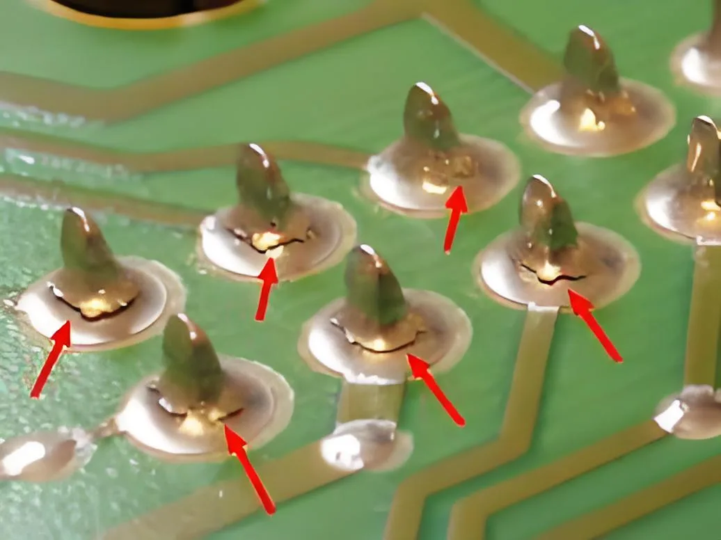

Prozessverbesserungen:
- Phosphorkontrolle: Verkürzen Sie die Lebensdauer des stromlosen Nickelbades, um den Phosphorgehalt zu erhöhen (High-P-Bereich).
- Nickeldicke: Halten Sie ≥4μm ein, um Lochfraß zu minimieren.
- Goldstärke: Beschränkung auf ≤0,1 μm mit verkürzter Eintauchzeit.
9. BGA-Lötstellenfehler: Mikrorisse und Spannungskonzentration
BGA-Verbindungen (0.4MM -Tonhöhe, 0.2mm Höhe) neigen bei Vibration oder Temperaturschock zu Mikrorissen. Ein Server HDI Fall gezeigt 300% Widerstandserhöhung nach Vibrationsprüfung.
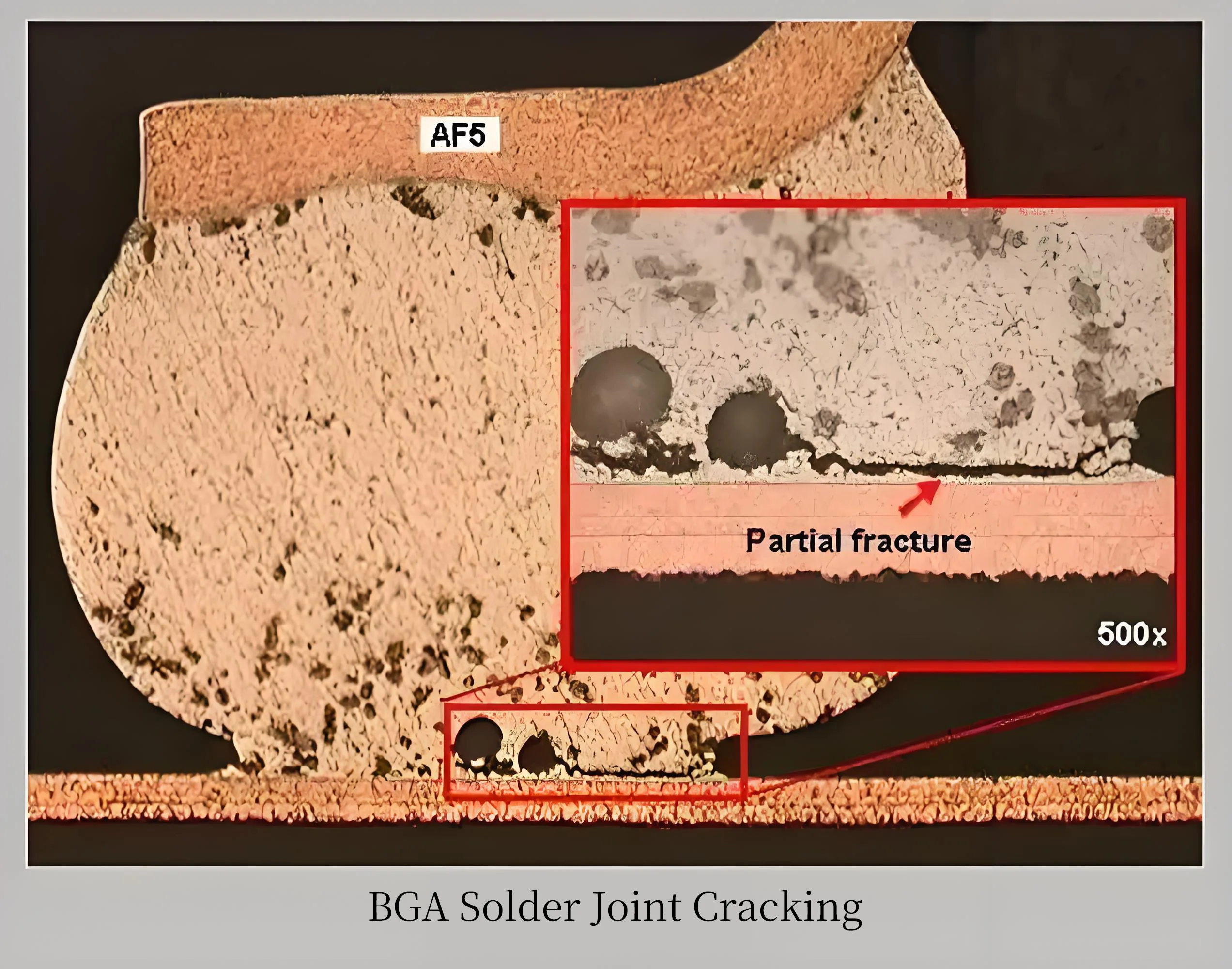

Lösungen:
- Layoutoptimierung: Vermeiden Sie eine falsche Platzierung der Kühlkörperschrauben, die die BGAs belasten.
- Biegekontrolle: Reduzieren Sie wiederholtes Biegen auf ein Minimum, um ein Abheben des Polsters zu verhindern.
- Materialabstimmung: Wählen Sie Substrate/Lote mit passendem CTE (z.B., FR-4 mit hoher Tg bei 8 ppm/°C vs. Standard 15 ppm/°C).
10. Unzureichendes thermisches Design: Komponentenkrise bei großer Hitze
Ein thermisch bedingter Komponentenausfall kommt häufig vor. A patented “blind-via PCB with integrated heat sink” enhances thermal performance via internal cavities and high-efficiency heat sinks, Schnelle Wärmeableitung und Reduzierung des Risikos thermischer Schäden.
Innovative Designmerkmale:
- Wärmehohlräume verbessern die Wärmeübertragung von der Senke zur Platine und die Gesamtkühlung.
- Kühlkörper absorbieren und verteilen die Wärme der Leiterplatte, Der Luftstrom leitet die Wärme effizient ab.
Übersichtstabelle als Referenz:
| Fehlertyp | Branchendurchschn. | Verbesserte Rate | Wichtige Steuerparameter |
|---|---|---|---|
| Kantenfehler | 2.2% | 0.1% | Bohrgenauigkeit 0,003 mm, 12h Akklimatisierung |
| THD-Falschlöten | 8.7% | 0.9% | Seitenverhältnis ≥1,5, Drei-Zonen-Temperaturregelung |
| Lochwand Kupfer | - - | IPC ≥20μm | Dickentoleranz ±1μm |
| Lotfüllrate | 68% | 93% | Dynamisches Profil: 280°C/3s + 380°C/2s |

Durch systematische Prozesskontrolle und -prävention können die meisten PCBA-Fehler gemindert werden. Die Zusammenarbeit mit erfahrenen Lieferanten und die Implementierung robuster Qualitätssysteme sind der Schlüssel zur Verbesserung der PCBA-Zuverlässigkeit. Für hochzuverlässige PCBA-Lösungen und technische Beratung, Kontakt uns heute.