

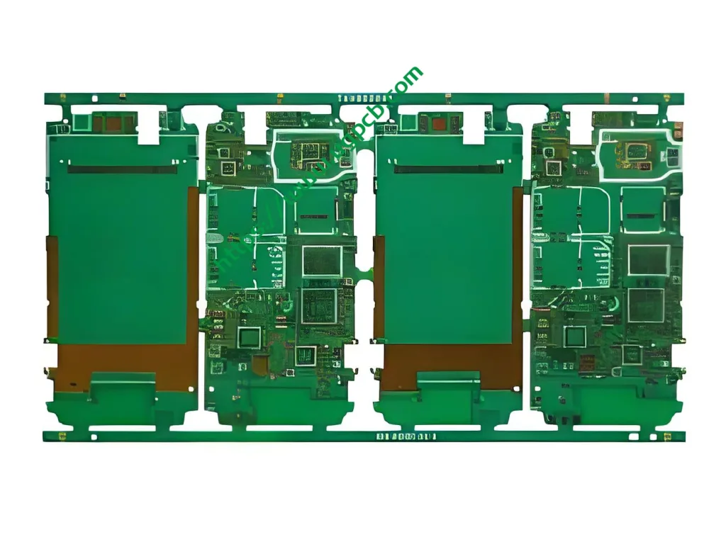
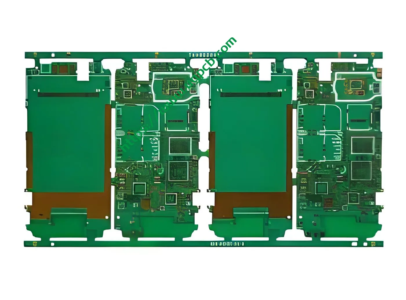
Overview of 6Layers PCB 1+N+1 HDI
The 6Layers PCB 1+N+1 HDI is a type of high – density interconnect printed circuit board. It plays a vital role in various electronic devices where space – saving and high – quality circuit connections are required.

Definition
“6Layers” indicates that this Leiterplatte has six layers in total. “1+N+1” represents a specific layer configuration, where “1” stands for a signal layer, “N” can be a combination of signal, Leistung, or ground layers in a flexible manner, and the last “1” is also a signal layer. “HDI” means High – Density Interconnect, which implies that it has a high density of electrical connections per unit area.
Entwurfsanforderungen
- Spur und Raum: The minimum trace and space is set at 3mil/3mil. This strict requirement ensures accurate circuit routing and minimizes the risk of electrical interference between adjacent traces.
- Hole Dimension: Mechanical holes should be no smaller than 0.2mm in diameter, and laser holes should be at least 0.1mm. These dimensions are crucial for proper component mounting and layer – to – layer connections.
Arbeitsprinzip
Electrical signals are transmitted through the copper traces on different layers. Vias are used to connect traces on different layers, enabling complex circuitry to be implemented within a compact space. The power and ground planes help to distribute power evenly and reduce electromagnetic interference.
Uses
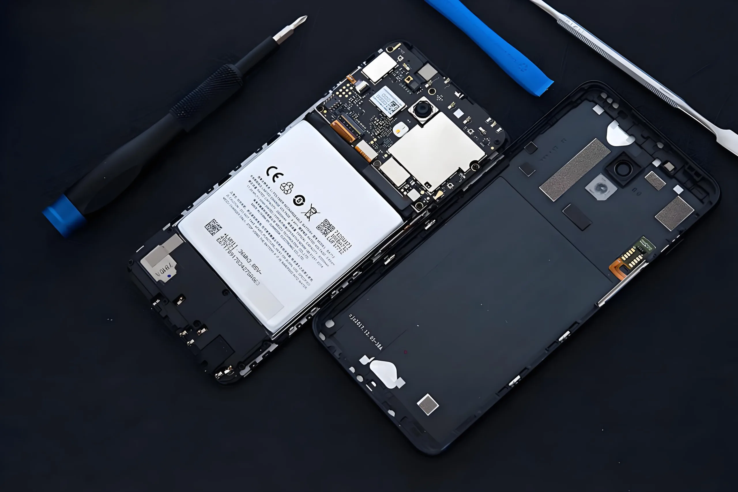
It is mainly used for mobile mainboard PCBs. In mobile phones, this PCB can handle multiple functions such as communication, Verarbeitung, and sensor integration due to its high – density layout.

Einstufung
It belongs to the multi – layer PCB category within the HDI PCBs. The 1+N+1 layer configuration is a distinct feature of its classification.
Material
The material is FR – 4. This material offers good mechanical strength, elektrische Isolierung, und Wärmewiderstand, which are essential for stable operation of electronic devices.
Leistung
- Elektrische Leistung: With inner copper thickness of 1OZ and outer 0.5OZ, it can effectively transmit electrical signals. The immersion gold surface treatment also has excellent electrical conductivity and promotes good solderability of components.
- Mechanical Performance: The FR – 4 base provides sufficient mechanical stability to withstand handling and installation in mobile devices.
Struktur
There are six layers in total. The two outer layers are typically used for signal or power/ground connections, and the “N” layer in the middle can be customized according to the specific circuit design needs.
Eigenschaften
- Compact Layout: Due to its high – density design, it allows more components to be accommodated in a smaller area.
- Good Surface Finish: The immersion gold treatment provides corrosion resistance and good solderability.
- Flexible Configuration: The 1+N+1 layer arrangement can be adjusted to meet different circuit design requirements.
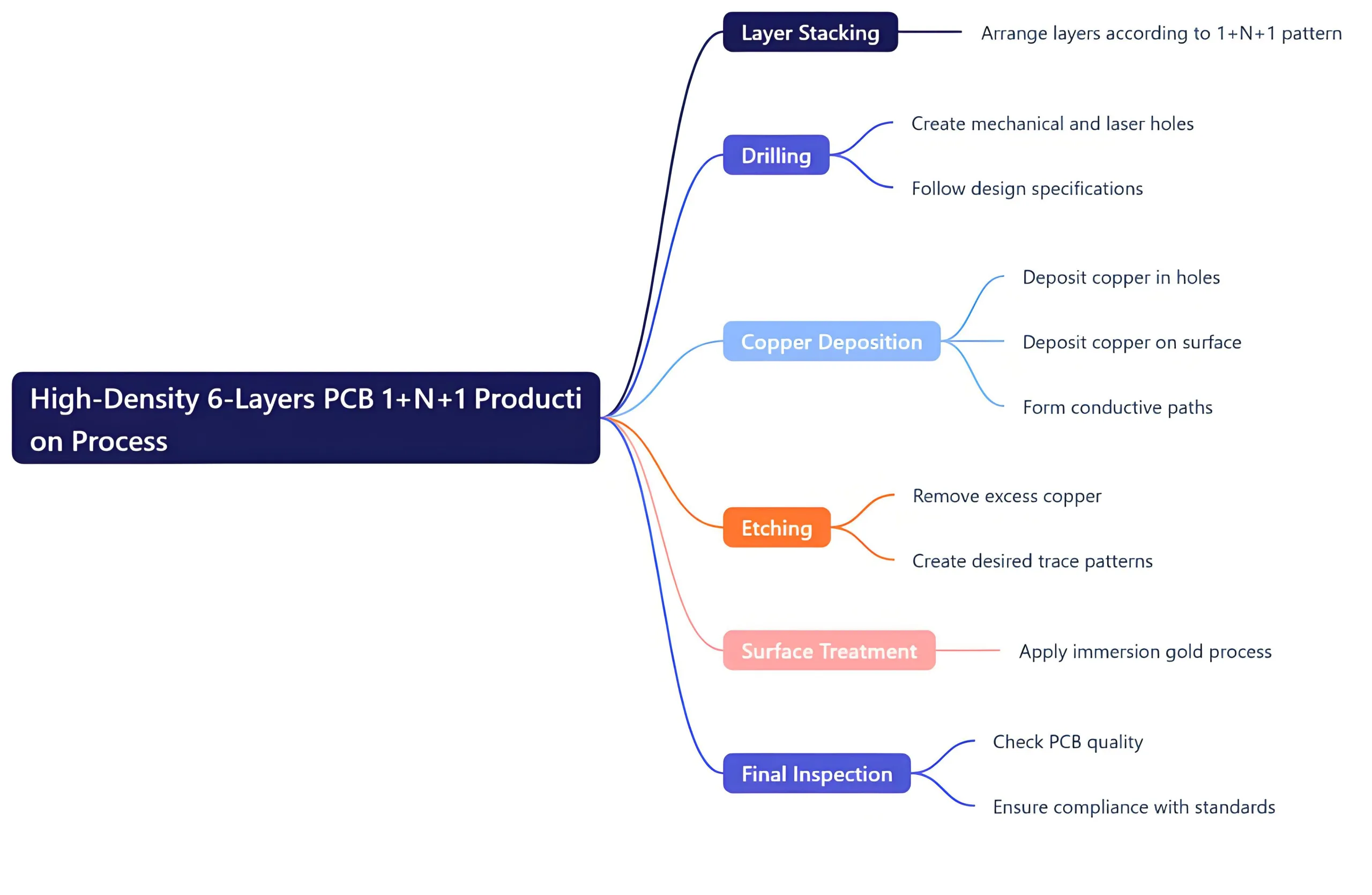
Produktionsprozess
- Schichtstapel: Arrange the six layers according to the 1+N+1 pattern accurately.
- Bohren: Create mechanical and laser holes as per the design specifications.
- Kupferablagerung: Deposit copper in the holes and on the surface to form conductive paths.
- Radierung: Remove excess copper to create the desired trace patterns.
- Oberflächenbehandlung: Apply the immersion gold process.
- Endinspektion: Check the PCB for quality and ensure it meets all standards.

Nutzungsszenarien
Apart from mobile mainboards, it can also be used in other small – form – factor electronic devices such as small portable media players or some compact Bluetooth devices where space is limited but reliable circuit connections are needed.