

8L 2+N+2 Mobile Main Board: Ein Überblick
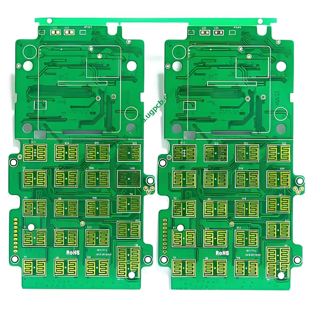
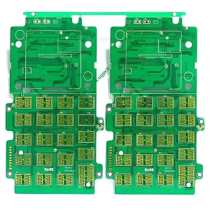
The 8L 2+N+2 Mobile Main Board is a high-density interconnect (HDI) Leiterplatte (Leiterplatte) designed specifically for mobile device applications. With its advanced construction and Materialien, this mainboard offers exceptional performance, Haltbarkeit, und Kompaktheit, making it ideal for modern smartphones and other portable electronics.

Key Specifications and Design Requirements
Material: The board is made from FR-4, a flame-retardant glass-reinforced epoxy laminate material that ensures excellent thermal and electrical performance.
Konstruktion: Der HDI technology allows for a complex eight-layer structure, with two core layers surrounded by alternating conductive and non-conductive layers, topped by additional conductive layers on the outermost sides. This configuration maximizes connectivity while minimizing space usage.
Fertige Dicke: The board has a standard finished thickness of 1.0mm, providing robustness without adding excessive bulk to the device.
Kupferdicke: A uniform copper thickness of 1oz across all layers ensures reliable signal transmission and power distribution.
Farboptionen: Erhältlich in Grün oder Weiß, catering to different aesthetic preferences or functional identification needs.
Oberflächenbehandlung: Immersion gold surface treatment enhances solderability and protects against corrosion, ensuring long-term reliability.
Minimale Spur/Platz: Capable of handling trace widths and spaces as fine as 3.5mil, enabling intricate circuit designs within limited spaces.
Minimum Hole: Supports both mechanical drilling down to 0.2mm and laser drilling down to 0.1mm, facilitating precise component placement.
Funktionsprinzip und Anwendungen
The working principle behind the 8L 2+N+2 Mobile Main Board involves optimizing signal paths and minimizing interference through strategic layering and advanced manufacturing techniques. This board is primarily used in mobile devices where size constraints are critical yet high performance is necessary. It serves as the central hub connecting various components such as processors, Speichermodule, power management units, and peripheral interfaces.
Classification and Usage Scenarios
Als HDI-Leiterplatte, the 8L 2+N+2 Mobile Main Board falls under the category of advanced circuit boards designed for high-performance electronic systems. Its primary application lies in the realm of mobile electronics, einschließlich:
- Smartphones, where it acts as the motherboard integrating multiple functions into a single, compact unit.
- Tablets and other portable computing devices requiring efficient power and signal management.
- Wearables and smart gadgets needing miniaturized yet powerful circuitry.
Production Process and Quality Control
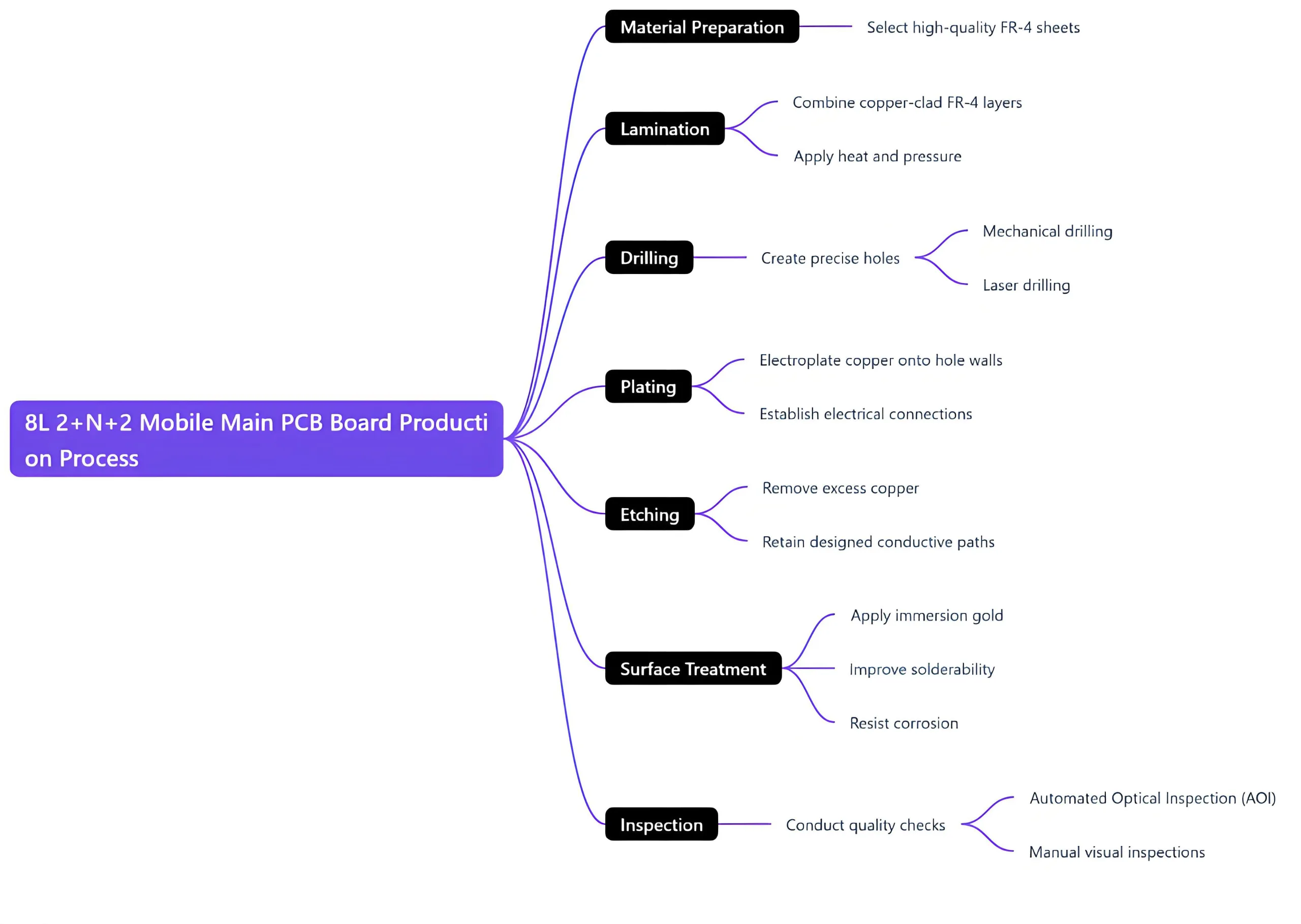

The production process begins with meticulous design using specialized software to optimize layout and ensure manufacturability. Key steps include:
- Materialvorbereitung: Selecting high-quality FR-4 sheets for the Grundmaterial.
- Laminierung: Combining multiple layers of copper-clad FR-4 under heat and pressure to form the desired structure.
- Bohren: Creating precise holes using both mechanical and laser drilling methods for component leads and interconnections.
- Überzug: Electroplating copper onto hole walls to establish electrical connections between layers.
- Radierung: Removing excess copper to leave only the designed conductive paths.
- Oberflächenbehandlung: Applying immersion gold to improve solderability and resist corrosion.
- Inspektion: Conducting rigorous quality checks throughout the process, including automated optical inspection (AOI) and manual visual inspections.
Abschluss
The 8L 2+N+2 Mobile Main Board represents a pinnacle of HDI PCB technology, tailored for the demands of modern mobile electronics. Its sophisticated design, coupled with premium materials and stringent manufacturing standards, ensures unparalleled connectivity, Zuverlässigkeit, and performance in a compact form factor. Whether integrated into the latest smartphone or innovative wearable tech, this mainboard empowers devices to deliver exceptional user experiences while maintaining sleek profiles.