

Model Overview
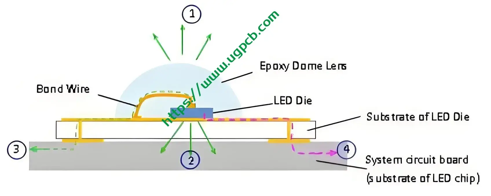
The LED Ceramic PCB and Ceramic Substrate PCB are advanced elektronische Komponenten designed for high-performance applications. Diese Leiterplatten feature a robust construction and superior thermal management capabilities, making them ideal for various demanding applications.

Materialzusammensetzung
The core of these PCBs is composed of a ceramic Substrat, which offers exceptional thermal conductivity and mechanical stability. The ceramic material used is primarily aluminum nitride (AlN), known for its high thermal conductivity and low electrical conductivity, making it an excellent choice for high-power electronics.
Ebenenkonfiguration
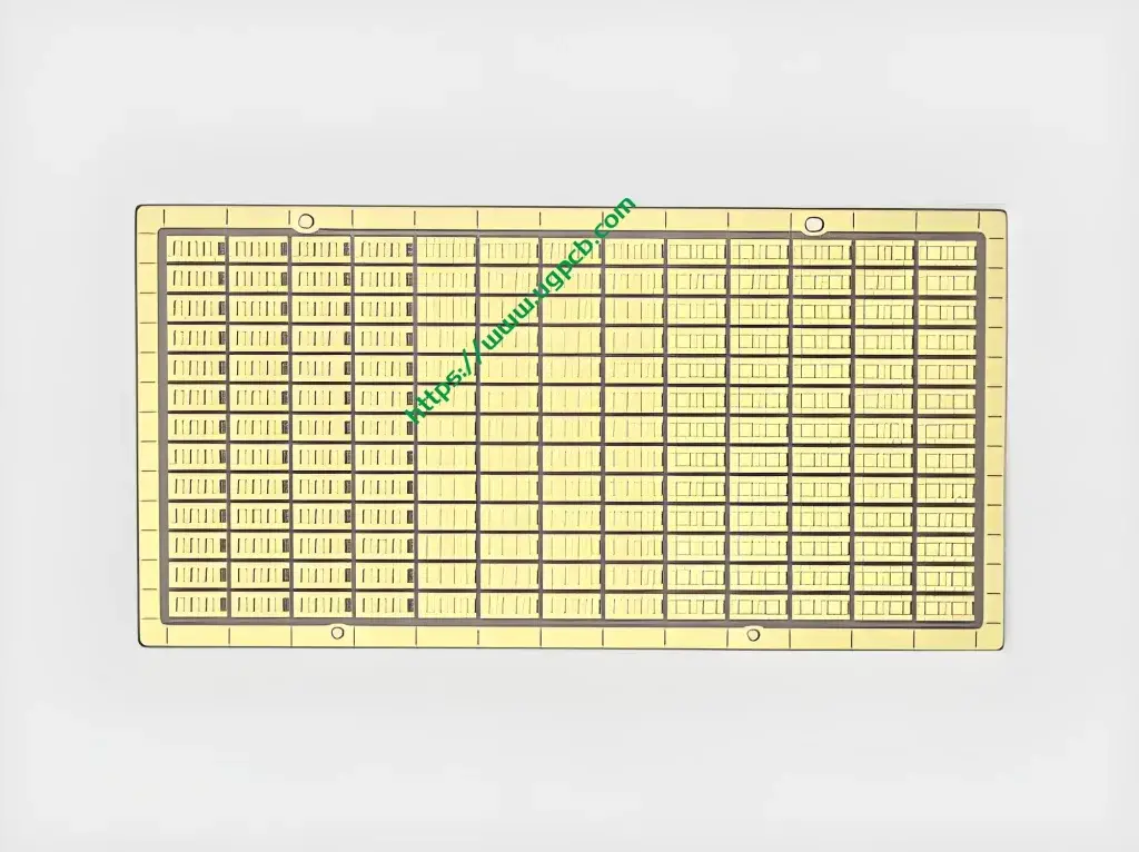
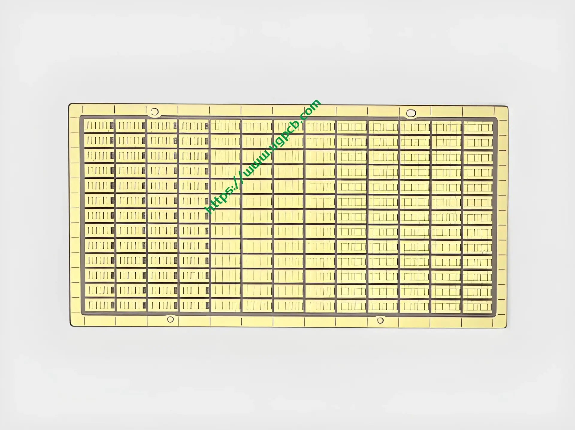
These PCBs are constructed as 2-layer ceramic PCBs, which means they have two layers of circuitry embedded within the ceramic substrate. This configuration allows for more complex circuit designs while maintaining the benefits of ceramic’s thermal properties.

Color and Appearance
The color of the LED Ceramic PCB and Ceramic Substrate PCB is white, giving them a sleek and professional appearance. The white ceramic surface also aids in reflecting light, which can be beneficial in certain applications.
Thickness Specifications
The thickness of the aluminum nitride ceramic substrate is precisely controlled at 0.635mm, ensuring consistent performance and reliability. This thickness provides a good balance between mechanical strength and thermal conductivity.
Kupferdicke
The copper thickness on these PCBs is 1OZ (35eins), which is sufficient for carrying high currents while maintaining good electrical conductivity. Die Kupferschicht ist geätzt, um die gewünschten Schaltungsmuster zu bilden.
Oberflächenbehandlung
The surface of the copper circuitry is treated with immersion gold, which provides excellent corrosion resistance and electrical conductivity. The gold thickness is >=3U”, ensuring reliable connections and long-term durability.
Minimale Blende
The minimum aperture size on these PCBs is 0.8mm, allowing for the use of small components and tight packaging layouts. This feature is crucial for high-density electronics applications.
Leistungseigenschaften
The LED Ceramic PCB and Ceramic Substrate PCB offer several performance characteristics that make them superior to traditional PCBs:
- Hohe Wärmeleitfähigkeit: The ceramic substrate effectively dissipates heat, preventing thermal buildup and component failure.
- Excellent electrical performance: The combination of ceramic and copper provides stable electrical properties, making these PCBs ideal for high-frequency and high-power applications.
- Mechanische Stabilität: The ceramic substrate is highly resistant to mechanical stress and vibration, ensuring reliable performance in harsh environments.
Produktionsprozess
The production of LED Ceramic PCBs and Ceramic Substrate PCBs involves several steps:
- Preparation of Ceramic Substrate: The ceramic material is processed to form the desired substrate shape and thickness.
- Circuit Design and Etching: The circuit patterns are designed and etched onto the copper layer using photolithography and etching techniques.
- Assembly and Lamination: The etched copper layers are assembled with the ceramic substrate, and the assembly is laminated to form a cohesive structure.
- Bohren und Plattieren: Holes are drilled for component placement, and the surfaces are plated with immersion gold to provide corrosion resistance and electrical conductivity.
- Endkontrolle und Tests: The finished PCBs are inspected for quality and tested to ensure they meet performance specifications.

Anwendungsszenarien
The LED Ceramic PCB and Ceramic Substrate PCB are ideal for a wide range of high-power applications, einschließlich:
- High-power LED lighting: These PCBs can handle the high currents and temperatures generated by high-power LEDs, making them suitable for LED lighting applications such as street lights, industrial lighting, and automotive headlights.
- Solar energy inverters: The high thermal conductivity of ceramic PCBs allows them to effectively dissipate heat generated by solar inverters, ensuring reliable and efficient operation.
- Other high-power electronics: These PCBs are also suitable for other high-power electronics applications, wie z.B. Netzteile, motor controllers, and battery management systems.
Abschließend, the LED Ceramic PCB and Ceramic Substrate PCB offer exceptional performance and reliability, making them ideal for high-power and high-performance electronics applications.