
High-Performance FR-4 Double-Sided PCB Descripción general del producto & Definición
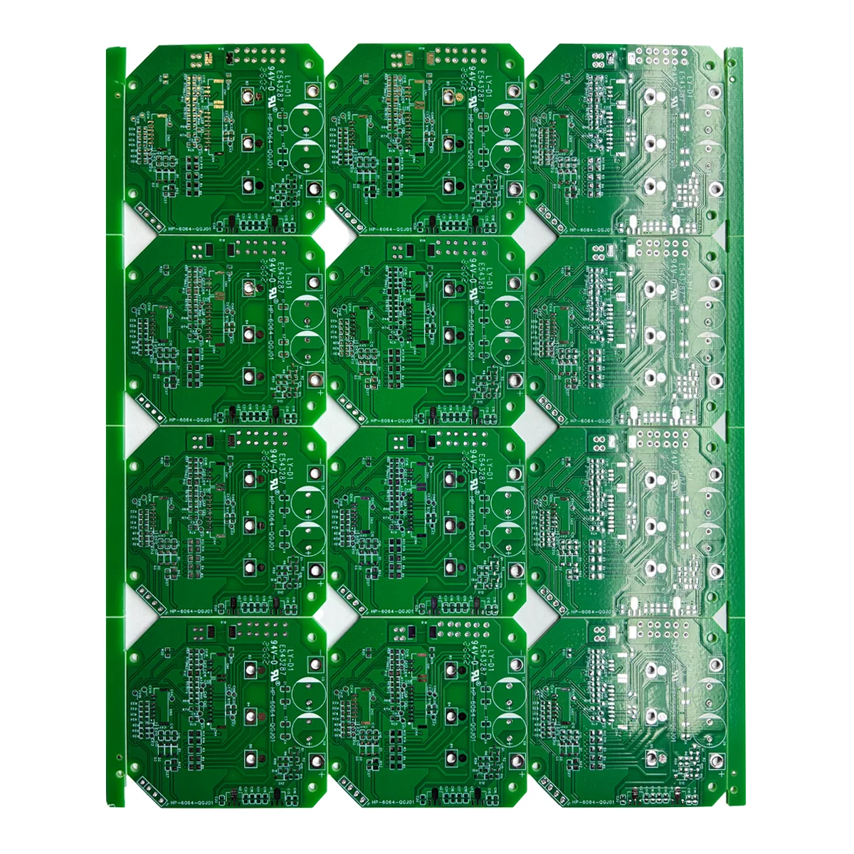
Este 2-Layer Rigid Placa de circuito impreso (tarjeta de circuito impreso) from UGPCB is a fundamental and widely used electronic interconnect solution. It features a standard 1.6mm de espesor del tablero, dimensions of 224.02mm x 189mm, and utilizes high-grade KB FR-4 laminate. This double-sided PCB serves as the essential “backbone” for electronic designs, providing reliable electrical connections and mechanical support for components. It is an ideal, cost-effective choice for a vast range of industrial control, electrónica de consumo, and power supply applications.

Consideraciones críticas de diseño
Successful design of a double-sided PCB requires balancing electrical performance with manufacturability. Key considerations include:
-
Routing Strategy: Efficiently utilize both top and bottom layers for trace routing. Plated Through-Holes (PTHs or Vias) enable inter-layer connections. La planificación cuidadosa de la densidad de trazas es crucial para evitar problemas de integridad de la señal como la diafonía..
-
Agujero & Diseño de almohadilla: Especifique tamaños de broca y diámetros de almohadilla apropiados para todos Vías de PCB y cables de componentes para garantizar resistencia mecánica y confiabilidad de soldadura., adhiriéndose a Normas IPC para anillo anular.
-
Fuerza & Planos de tierra: Mientras que los aviones dedicados están ausentes, Los diseñadores deben ampliar las líneas de alimentación y tierra o implementar un vertido de cobre enrejado para reducir la impedancia y mejorar la estabilidad, un aspecto clave de una robustez. diseño de PCB.
-
Verificación de reglas de diseño (República Democrática del Congo): Antes de la fabricación, verificar rigurosamente que todos los parámetros (ancho/espacio libre de traza, tamaños de agujeros) alinearse con las capacidades del fabricante (según las especificaciones de esta placa) garantizar Diseño de PCB para capacidad de fabricación (DFM).
Principio de trabajo & Estructura
La funcionalidad de este placa de circuito de doble capa proviene de su estructura en capas:
-
Construcción: El núcleo está formado por un Capa dieléctrica aislante FR-4, revestido con lámina de cobre (típicamente 1 onz) en ambos lados. El cobre no deseado se elimina durante fabricación de PCB, formando las trazas del circuito deseado.
-
Interconexión Eléctrica: Los circuitos de las dos capas están conectados verticalmente mediante Plated Through-Holes (PTH), creado a través de perforación mecánica seguido por Deposición de cobre no electrolítica y electrolítica..
-
Protección de superficies: El Nivelación de soldadura por aire caliente sin plomo (HASL) El acabado aplicado a las almohadillas de cobre expuestas previene la oxidación y garantiza una excelente soldabilidad para el ensamblaje de componentes..
Clasificación de productos & Materiales
Según las especificaciones proporcionadas, Este producto está clasificado con precisión de la siguiente manera.:
-
Por recuento de capas: PCB de doble cara o 2-PCB de capa.
-
Por rigidez del sustrato: PCB rígido.
-
Por material base: FR-4 PCB. Específicamente, FR-4 from the “KB” brand, un laminado de vidrio epoxi conocido por su aislamiento eléctrico superior, resistencia mecánica, y retardante de llama (UL94-V0).
-
Por acabado superficial: PCB HASL sin plomo.
-
Por complejidad de la aplicación: Estándar, PCB de uso general y grado industrial.
Actuación & Características clave
Aprovechar los materiales y procesos especificados., Esta PCB ofrece los siguientes beneficios de rendimiento principales:
-
Mecánica confiable & Rendimiento eléctrico: El Material KB FR-4 Ofrece una constante dieléctrica estable y un factor de disipación bajo para la integridad de la señal.. El espesor estándar de 1,6 mm proporciona una excelente resistencia a la flexión y la vibración..
-
Interconexiones confiables: El Acabado superficial HASL sin plomo proporciona un piso, Recubrimiento altamente soldable compatible con procesos de soldadura por ola y soldadura manual..
-
Estabilidad térmica superior: El sustrato FR-4 resiste temperaturas de soldadura estándar y ofrece una alta temperatura de funcionamiento continuo, adecuado para la mayoría electronica industrial entornos.
-
Alta rentabilidad: En comparación con los tableros multicapa, PCB de doble cara oferta significativamente menor Costo de fabricación de PCB y plazos de entrega más cortos, representando una solución de hardware económica.
-
Cumplimiento ambiental: El HASL sin plomo El proceso cumple con directivas internacionales como RoHS..
Proceso de fabricación detallado
UGPCB se adhiere a un estricto, alto nivel Proceso de fabricación de PCB:
-
Ingeniería & LEVA: Análisis de archivos Gerber, verificación DFM, y generación de fotogramas.
-
Panelización: Cortando el FR-4 grande laminado revestido de cobre en paneles de producción.
-
Perforación: Perforación CNC de orificios de componentes y Vías de PCB.
-
Metalización de agujeros: desmechar, deposición química de cobre, y revestimiento de cobre electrolítico para formar conductores Plated Through-Holes (PTH).
-
Patrones: Aplicando fotorresistente, exposición, desarrollo para transferir la imagen del circuito.
-
Aguafuerte: Eliminación de cobre no deseado para formar trazas de circuito precisas.
-
Máscara de soldadura & Platina: Aplicar máscara de soldadura LPI (típicamente verde) e impresión de leyendas.
-
Acabado superficial: Aplicando HASL sin plomo revestimiento de almohadillas expuestas.
-
Enrutamiento & Prueba eléctrica: Perfilado hasta el esquema final del tablero y realización de pruebas eléctricas. (Sonda voladora o prueba de fijación).
-
Inspección final & Embalaje: Integral Inspección óptica automatizada (AOI), verificación dimensional, y sellado al vacío, embalaje a prueba de humedad.
Aplicaciones primarias & Casos de uso
Esta especificación de PCB FR-4 de doble cara se implementa ampliamente en fiable y económico aplicaciones:
-
Sistemas de control industriales: Controladores PLC, tableros de accionamiento de motor, módulos de interfaz de sensores.
-
Unidades de fuente de alimentación: Fuentes de alimentación conmutadas (SMPS), Sistemas UPS, Placas de controladores LED.
-
Electrónica de Consumo: Tableros de control de electrodomésticos (C.A., lavadoras), controladores domésticos inteligentes, equipo de audio.
-
Electrónica automotriz: Módulos de control de carrocería (BCM), controladores de iluminación, sistemas de infoentretenimiento no críticos.
-
Equipos de telecomunicaciones: Módulos funcionales dentro de los enrutadores., interruptores.
-
Prueba & Instrumentos de medición: Paneles de adquisición y visualización de datos para equipos..


¿Por qué elegir UGPCB para sus necesidades de PCB de doble cara??
Asociarse con garantías UGPCB:
-
Fabricación de precisión: Cumplimiento estricto del espesor de 1,6 mm, 224.02dimensiones x189mm, y Material FR-4 presupuesto.
-
Excelencia en los procesos: Estandarizado Producción de PCB HASL sin plomo garantiza consistencia y confiabilidad entre lotes.
-
Soporte técnico experto: Nuestro equipo brinda soporte integral., de diseño de PCB revisar a la consulta de producción.
-
Entrega rápida llave en mano: Ofrecemos plazos de entrega competitivos para doble capa estándar. prototipos de PCB y tiradas de producción.
Listo para iniciar tu proyecto? Póngase en contacto con UGPCB hoy para obtener una cotización competitiva y soporte experto. Seamos tu confianza fabricante de PCB y socio para el éxito.