


Introducción a la PCB de carga inalámbrica
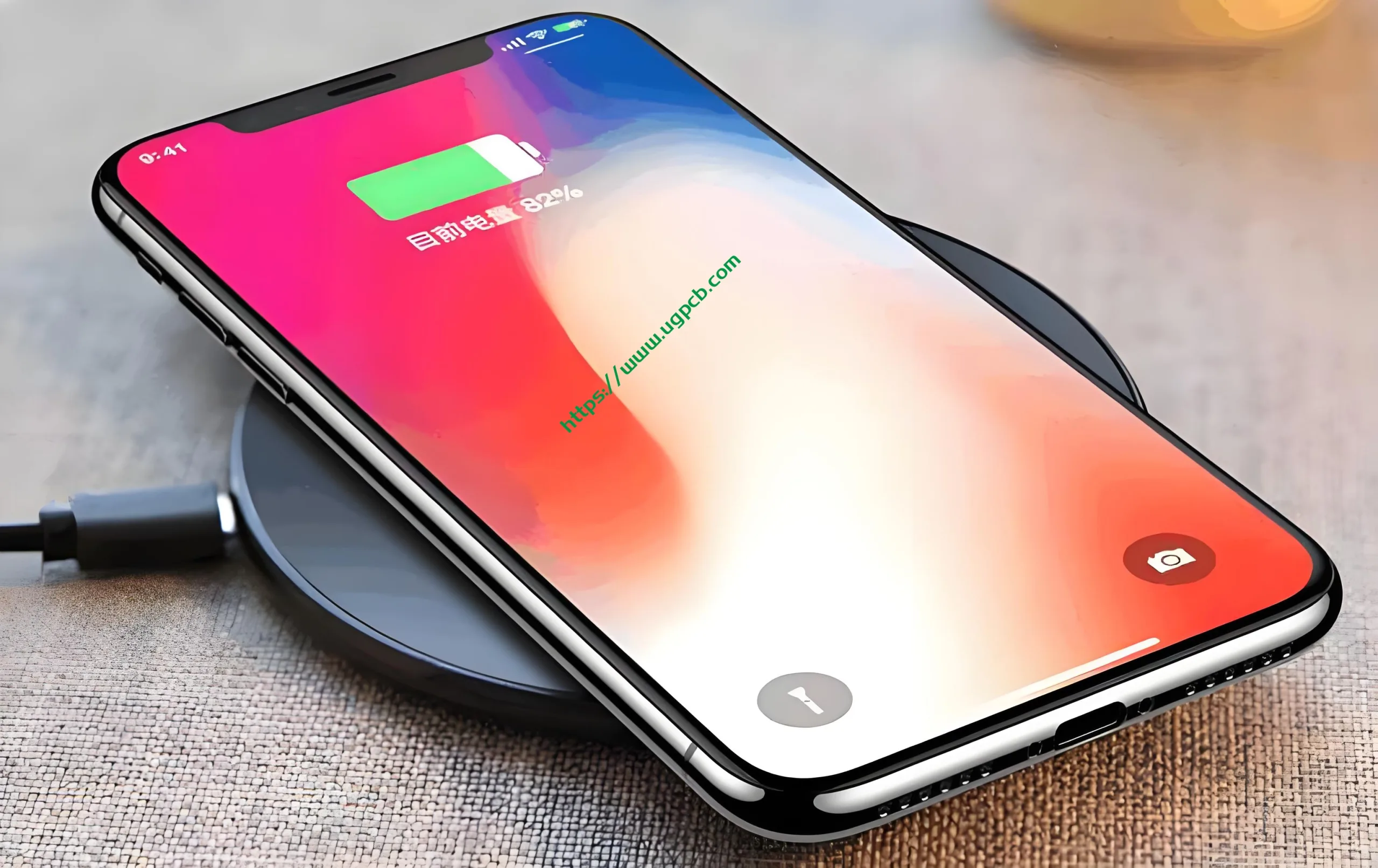
Una PCB de carga inalámbrica, También conocido como carga inductiva. tarjeta de circuitos, Es una placa de circuito impreso especializada diseñada para la transferencia de energía inalámbrica.. Permite que dispositivos como teléfonos inteligentes, tabletas, y otros aparatos electrónicos para cargar sin necesidad de conectores físicos.

Principio de trabajo
La tecnología de carga inalámbrica funciona según el principio de inducción electromagnética.. La bobina transmisora genera un campo electromagnético alterno que induce una corriente en la bobina receptora., transfiriendo así energía del cargador al dispositivo.
Aplicaciones
Los PCB de carga inalámbrica se utilizan ampliamente en productos electrónicos de consumo para cargar dispositivos como teléfonos móviles., relojes inteligentes, auriculares, e incluso cepillos de dientes eléctricos. Ofrecen comodidad, facilidad de uso, y menor desgaste en los puertos de carga.

Tipos de PCB de carga inalámbrica
Hay dos tipos principales de tecnologías de carga inalámbrica.:
- Estándar Qi: El estándar de carga inalámbrica más común y ampliamente adoptado.
- AMP (Alianza de Asuntos de Poder): Otro estándar popular, A menudo se encuentra en dispositivos más antiguos..
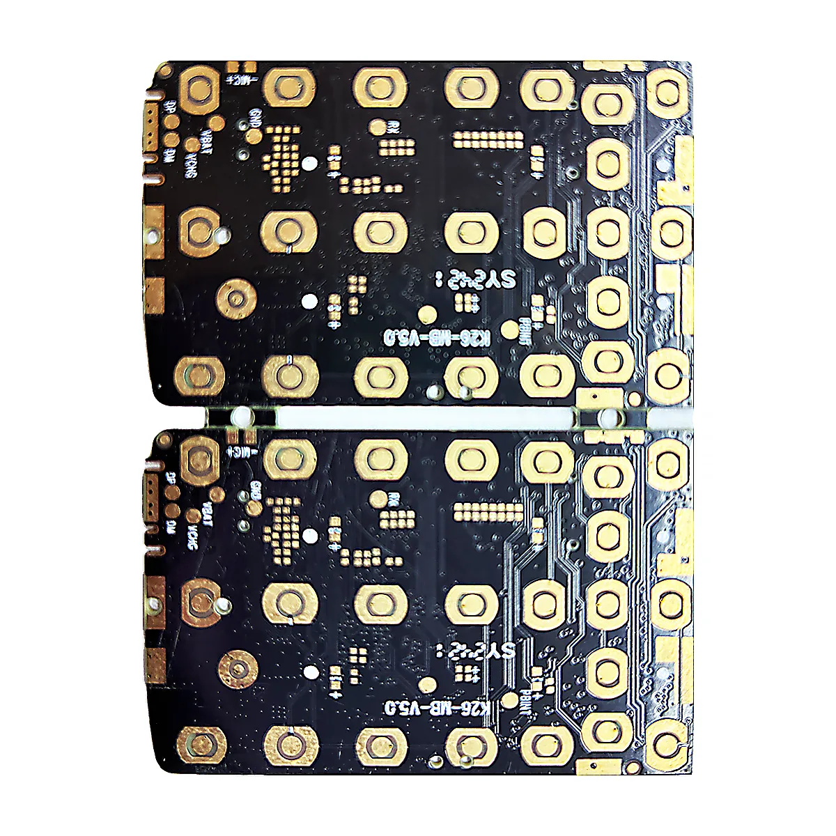
Material y construcción
- Material: S1000-2, un material epoxi de alta calidad.
- capas: 6 capas, proporcionando robustez y una mejor integridad de la señal.
- Color: Disponible en verde o blanco.
- Espesor terminado: 1.2milímetros, asegurando durabilidad y al mismo tiempo siendo delgado.
- Espesor de cobre: 2ONZ, que ofrece buena conductividad.
- Tratamiento superficial: Immersion gold with a thickness of at least 2U”, mejorando la resistencia a la corrosión y la soldabilidad.
- Espesor de cobre en el agujero: 35UNO, asegurando conexiones fuertes.
- Apertura mínima: 0.4milímetros, permitiendo un trabajo de detalles finos.
Características de rendimiento
Los PCB de carga inalámbrica están diseñados para transferir energía de manera eficiente con una pérdida mínima. Admiten capacidades de carga rápida y están diseñados para resistir el uso repetido a lo largo del tiempo.. El acabado dorado por inmersión garantiza un rendimiento y una fiabilidad duraderos..
Características estructurales
La estructura de una PCB de carga inalámbrica incluye múltiples capas de trazas de cobre intercaladas entre capas de material de sustrato.. Este diseño multicapa ayuda a gestionar la disipación de calor y mejorar el rendimiento eléctrico.. El tarjeta de circuito impreso está recubierto con una capa protectora para evitar daños y garantizar la longevidad.
Proceso de producción
La producción de una PCB de carga inalámbrica implica varios pasos:
- Diseño: Usar software especializado para crear el diseño del circuito..
- Aguafuerte: Quitar el exceso de cobre para formar los patrones deseados..
- Laminación: Combinando varias capas juntas.
- Enchapado: Agregar una fina capa de metal para mejorar la conectividad.
- Inspección: Garantizar que la PCB cumpla con los estándares de calidad.
- Asamblea: Montaje de componentes en la PCB.
- Pruebas: Verificación de funcionalidad y rendimiento.

Casos de uso
Los PCB de carga inalámbrica se utilizan en diversas aplicaciones, incluidas:
- Electrónica de Consumo: Teléfonos móviles, tabletas, relojes inteligentes.
- Automotor: Sistemas de carga para smartphones en el coche.
- Dispositivos médicos: Equipo médico portátil.
- Wearables: Rastreadores de actividad física, anillos inteligentes.
En conclusión, Los PCB de carga inalámbrica representan un avance significativo en la tecnología de carga, ofreciendo comodidad, eficiencia, y durabilidad. Su adopción generalizada en diferentes industrias resalta su versatilidad e importancia en los dispositivos electrónicos modernos..