

Percée révolutionnaire en électronique flexible
Dans les plis gracieux des écrans de smartphone et les mouvements précis de Mars Rover Arms, cartes de circuits imprimés flexibles (FPCBS) conduisent tranquillement la troisième révolution en électronique. Selon les données de prismark, Le marché mondial du FPCB a dépassé $120 milliards dans 2023, avec un taux de croissance annuel composé (TCAC) de 8.7%. Cette technologie innovante, combinant conducteurs avec des films diélectriques flexibles, redéfinit la forme physique et les limites fonctionnelles des appareils électroniques.
je. La taxonomie des circuits flexibles
1.1 L'art de l'harmonie rigide-flex
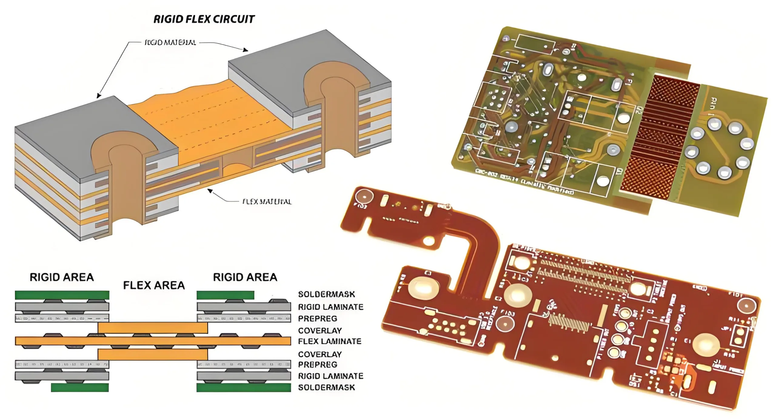

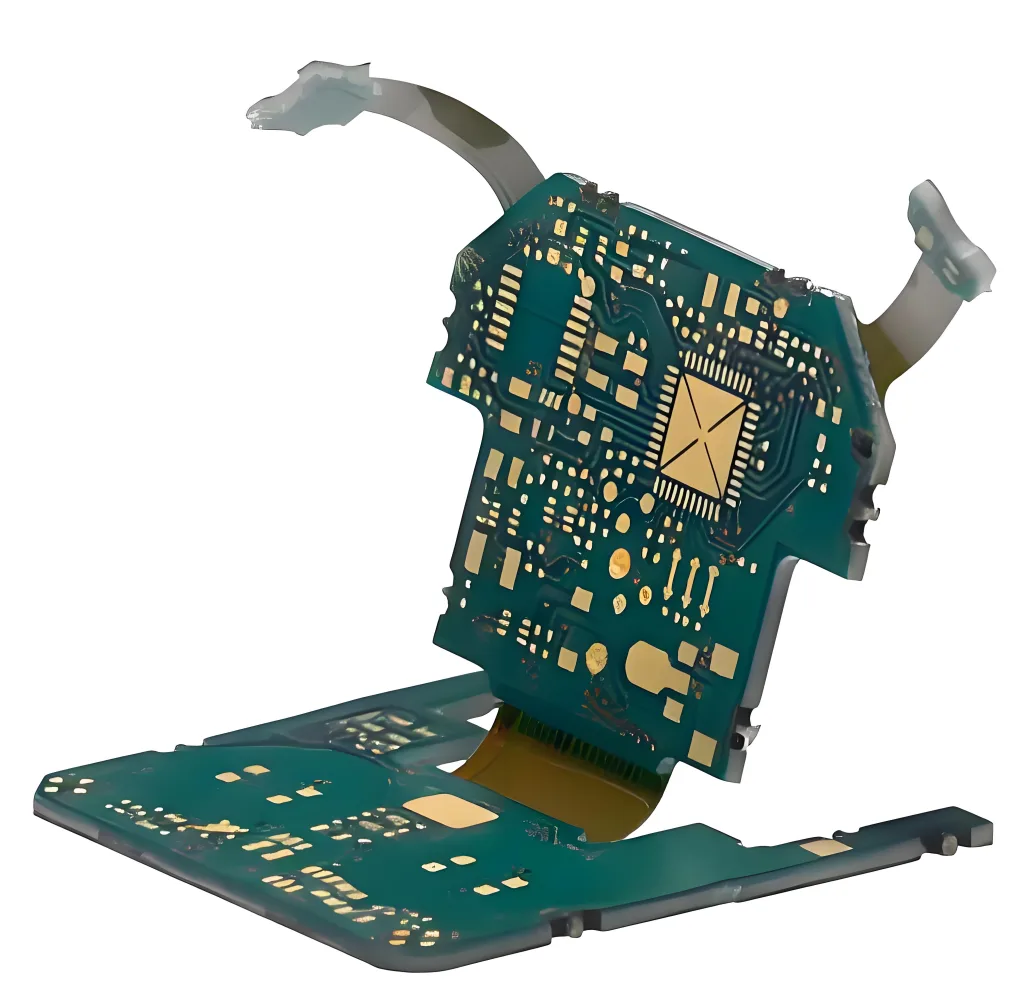
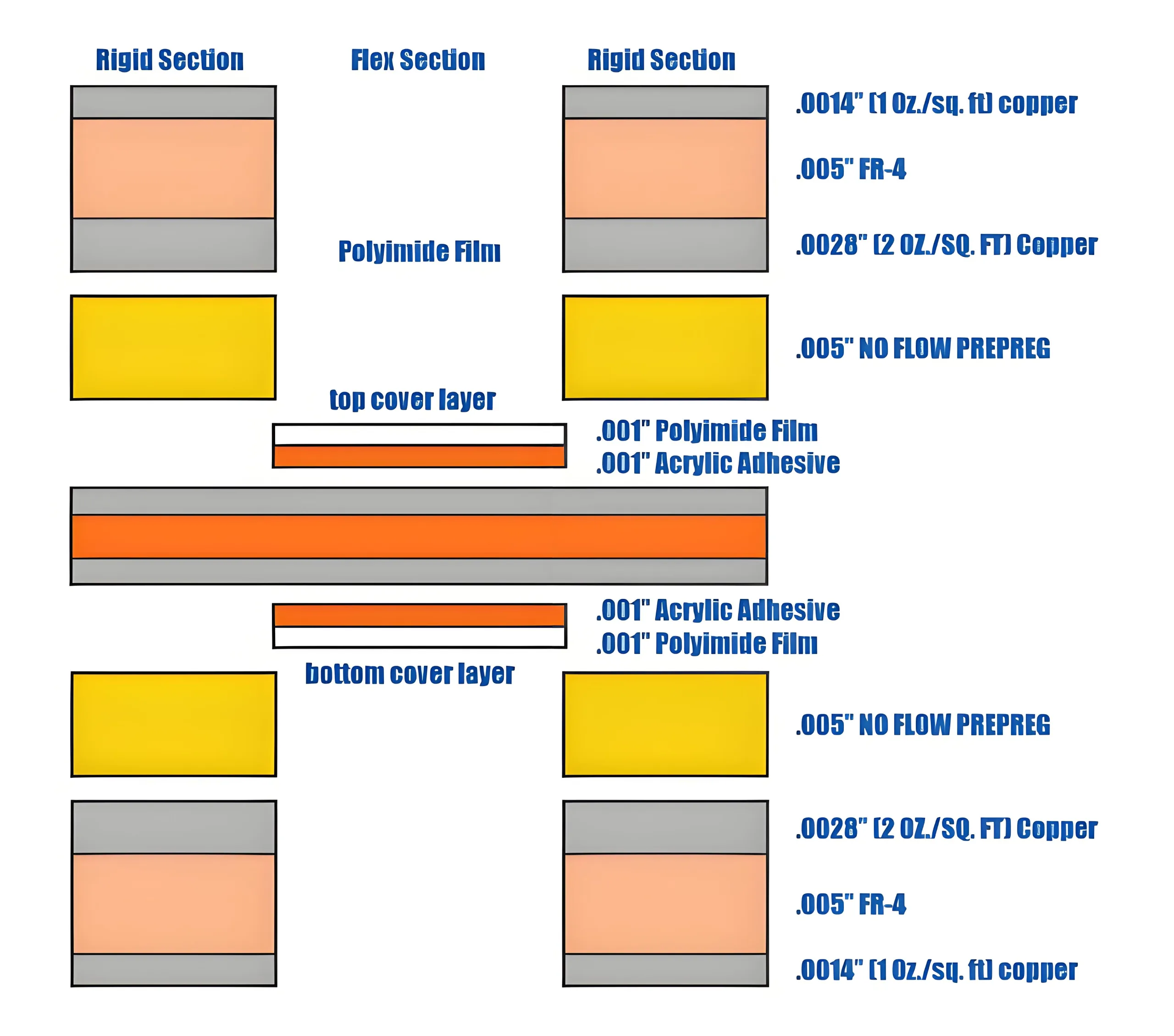
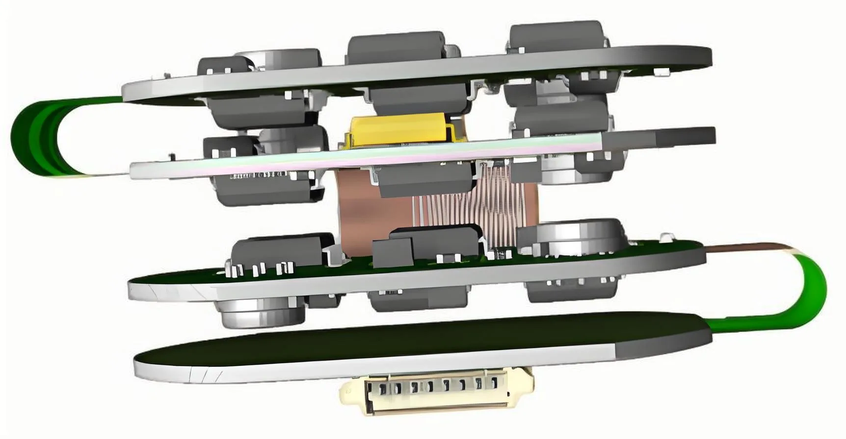
Les circuits flexibles se répartissent en deux catégories: Circuits flexibles purs (FPC) et hybrides flex rigides. Le premier, Aussi mince que les ailes de la cigade (0.1–0,3 mm), Emploie des substrats en plastique flexibles, tandis que ce dernier fusionne des sections FR4 rigides avec des zones flexibles en polyimide utilisant des résines époxy. En smartphones, Les conceptions rigides-flex permettent un rayon de flexion aussi petit que 3 mm (Formule: R_min = 100 × t, où t = épaisseur du matériau), Connecter de manière transparente les tableaux principaux aux écrans.
1.2 Sélection stratégique entre les applications statiques et dynamiques
- Applications statiques: Circuits de tableau de bord automobile (<100 virages annuels) Utilisez des structures en cuivre roulées à 3 couches avec de 18 μm de papier.
- Applications dynamiques: Les circuits de charnière d'ordinateur portable nécessitent >1 Million Bend Cycles, cuivre électrique à 2 couches exigeant avec armature en acier.

II. Le jeu de précision de la science matérielle
2.1 Évolution des matériaux de substrat
Polyimide (PI) Les films dominent les applications haut de gamme avec une température de transition en verre (Tg) de 260 ° C et module élastique de 16 GPA. Polymère de cristal liquide émergent (LCP) matériels, en vedette 0.2% Absorption de l'humidité et >10 Performance à haute fréquence GHZ, révolutionnent les applications 5G MMWAVE.
2.2 La bataille à l'échelle micron des feuilles de cuivre
Le choix entre roulé recuit (Rampe) et électrodeposité (Élégant) Les feuilles de cuivre impliquent des compromis critiques:
- Fleuret britannique: 20% allongement pour la flexion dynamique
- Fleuret Ed: 30% Réduction des coûts pour une utilisation statique
L'analyse XRD révèle (220) L'orientation du plan de cristal varie 85%, Expliquer sa ductilité exceptionnelle.
III. Stratégies de conception multidimensionnelles
3.1 Optimisation de topologie d'empilement
Dans les modules radar autonomes, engineers adopt a “2-2-2” stackup: 6-Le routage des calques dans des zones rigides et les couches de signal L2 / L5 conservées dans des zones flexibles. Cela limite la variation constante diélectrique à ± 5% dans les zones de pliage, garantissant 77 Intégrité du signal GHZ.

3.2 Twin numérique de Bend Mechanics
Analyse par éléments finis (Fea) Modèles pliant le stress en utilisant:
S_max = (E × t)/(2R.)
Où E = module élastique, t = épaisseur, R. = rayon de pliage. Déformation en cuivre dépassant 0.3% déclenche des optimisations de renforcement ou de routage.
IV. Briser les limites de la fabrication
4.1 L'art du pliage 3D
Les simulations multiphysiques mécaniques ANSYS doivent tenir compte:
- Distribution mécanique des contraintes
- Correspondance CTE (Pi Material CTE ≈15 ppm / ° C)
- Stabilité de phase à haute fréquence
4.2 Règles d'or de conception pour la fabrication
- Pas de vias dans les zones de virage (autorisation >3 mm)
- “10-Degree Rule” for conductor angles between adjacent layers
- Formule d'ouverture de la couverture: D_pad = d_solder + 0.1 mm

V. Futures frontières: Le nouvel horizon de l'électronique flexible
Dans les appareils métaverse, FPCBS transcende les formes traditionnelles. Les circuits imprimés en 3D du MIT réalisent 500% déformation de traction, Alors que les variantes biodégradables de Stanford sont prometteuses dans la technologie médicale implantable. Avec un rouleau (R2R) Fabrication de réduction des coûts par 8% annuellement, une époque intelligente entièrement flexible Dawns.
Épilogue: Équilibrer la rigidité et la flexibilité pour demain
Des modules lunaires Apollo aux smartphones pliables, Les FPCB ont évolué 60 Des années des merveilles aérospatiales aux éléments essentiels quotidiens. Circuits de gravure sur des films de polyimide de 0,1 mm écrit une épopée industrielle à des échelles microscopiques. Ce champ dynamique attend les ingénieurs pour redessiner l'avenir de l'électronique le long de la frontière philosophique entre la rigidité et la flexibilité.