
UGPCB 18-Layer Server PCB: Engineered for High-Performance Computing & Centres de données
In the era of data centers and cloud computing, server stability and performance are critical to digital business operations. As the fundamental hardware carrier, the precision design and exceptional quality of Server PCB (Cartes de circuits imprimés) are paramount. Leveraging deep industry expertise and cutting-edge technology, UGPCB provides high-performance, highly reliable 18-layer server PCBs to meet the most demanding requirements of next-generation data center applications.

Présentation du produit & Définition
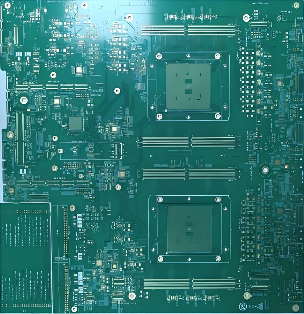
A server PCB is the core component of server motherboards, storage backplanes, and various functional daughter cards. It hosts critical components like CPUs, mémoire, and chipsets, facilitating high-speed signal transmission, distribution d'énergie, and system interconnection. Designed specifically for high-performance application servers, this UGPCB product utilizes an 18-layer high multilayer structure and an enhanced board thickness of 2.4mm ±10%, serving as a robust hardware foundation for processing massive datasets and supporting high-speed computations.
Core Design Highlights & Technical Analysis
To address server platforms’ extreme demands for signal integrity, intégrité de puissance, et gestion thermique, this product integrates several key technologies:
-
Advanced Stack-up & Matériels:
-
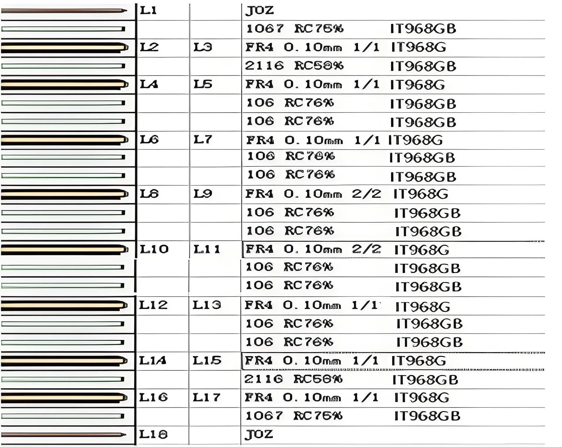
Stratifié: Utilizes ITEQ IT968G high-speed, low-loss material. Its high Tg (Température de transition du verre) ensures dimensional stability and consistent electrical performance under prolonged high-temperature server operation, effectively reducing signal transmission loss.
-
Calques & Poids du cuivre: An 18-layer complex stack-up with a meticulously designed hybrid copper weight scheme (featuring 2Oz thick copper foil on select inner layers). This optimizes the current-carrying capacity and thermal performance of power planes while enabling fine-line routing on high-speed signal layers.
-
-
Precision Routing & Interconnection:
-
Line Capability: Achieves ultra-fine line width/space of 0.1mm/0.1mm, meeting the fan-out and interconnection requirements for high-density BGA packages (par ex., Processeur, GPU, FPGA).
-
Technologie microvia: Supports a minimum mechanical drill diameter of 0.20mm, enhancing routing density and space utilization.
-
-
Key Technologies for Signal Integrity:
-
Back-Drilling: For high-speed differential signals (par ex., Pie, Sas, Ethernet), the back-drilling process removes unused copper stubs from through-holes, significantly reducing signal reflection and attenuation. This is a core process for ensuring signal quality in PCB à grande vitesse.
-
RTF Copper Foil: Uses Reverse Treated Foil, which provides a smoother copper surface. This effectively reduces skin effect loss for high-frequency signals, improving signal transmission efficiency.
-
-
Finition de surface fiable:
-
Or par immersion au nickel autocatalytique (ACCEPTER) is applied as the final surface treatment. ENIG provides a flat surface, excellente soudabilité, a reliable contact interface, and long-term oxidation resistance, making it ideal for soldering dense, fine-pitch composants on server PCBs.
-
Product Features & Avantages
-
Exceptional Electrical Performance: High-speed IT968G laminate combined with back-drilling and RTF foil ensures low-loss, low-latency transmission of high-frequency signals, making it an ideal choice for PCB haute fréquence et PCB à grande vitesse.
-
Superior Power Handling & Gestion thermique: 2Oz inner-layer copper and the 2.4mm board design enhance current-carrying capacity, overall structural rigidity, and thermal conductivity.
-
Densité élevée & Fiabilité: The 18-layer routing space coupled with 0.1/0.1mm line width/space supports the most complex designs. Strict process control and high-Tg materials ensure long-term reliability for 24/7 uninterrupted operation.
-
End-to-End Service Support: UGPCB offers not only top-tier Fabrication de PCB but also a one-stop solution from design review to production, accélérant votre time-to-market.
Aperçu du processus de production
Our manufacturing adheres to stringent Normes IPC and a quality management system:
Engineering Review → Material Preparation → Inner Layer Imaging → Lamination → Drilling & Back-Drilling → Hole Metallization → Outer Layer Imaging → Plating (for hybrid copper weight) → Application du masque de soudure (Pre-ENIG) → ENIG → Routing / Profiling → Electrical Test & Inspection finale
https://via.placeholder.com/800×450.png?text=18-Layer+PCB+Cross-Section
Alt Text: Cross-sectional view of an 18-layer server PCB board, detailing precise lamination and back-drilled via structures for high-speed signal transmission.
Applications & Classification
This high-performance PCB is widely used in:
-
Enterprise & Cloud Server Motherboards
-
Data Center AI Computing Acceleration Cards
-
High-Performance Storage Servers & Fonds de panier
-
Network Switch & Communication Equipment Core Boards
Classement Technique:
-
Par nombre de couches: Haut PCB multicouche (18 Calques)
-
Par technologie: High-Speed/High-Frequency PCB, Back-Drilled PCB, PCB en cuivre lourd
-
Par candidature: Server/Data Center PCB
-
Par finition de surface: ACCEPTER (Or par immersion au nickel autocatalytique) PCB
Choisissez UGPCB, and you select more than just a high-quality server PCB board; you gain a trusted partner in advanced PCB manufacturing. We are dedicated to translating complex technical details into reliable advantages for your products, empowering your next-generation data center solutions.
Contact our expert team today for a customized PCB solution quote and technical consultation!


