
UGPCB: In che modo la progettazione PCB convenzionale e di precisione alimenta l'innovazione elettronica globale
Ad un drone di Shenzhen R&Centro D, Engineer Wang faced EMI test failures on the 7th flight controller PCB iteration – where minor RF interference caused system malfunction. Dopo aver coinvolto il team di UGPCB, ottimizzazione dello stack-up E ricostruzione della strategia di grounding integrità del segnale potenziata da 40%, accelerare il lancio del prodotto di due mesi. Questo caso reale dimostra come La progettazione professionale dei PCB determina il successo dei prodotti elettronici.
Valore fondamentale e competenza tecnica nella progettazione PCB convenzionale
PCB convenzionali (2-16 strati) rimangono la spina dorsale del settore, presa 75% quota di mercato globale (Prismark 2023). L'eccellenza tecnica si manifesta in tre dimensioni:
-
Controllo dell'integrità del segnale
Per le frequenze >100MHz, IL formula dell'impedenza caratteristica Z₀ = 87/√(εᵣ+1.41) × ln(5.98H/(0.8W+T.)) diventa critico. Gli ingegneri UGPCB mantengono una tolleranza di impedenza di ±7%. (superando lo standard ±10% di IPC-6012B) grazie alla precisa larghezza della microstriscia (W), spessore dielettrico (H), e peso in rame (T) calcoli. -
Ingegneria della gestione termica
Segue un aumento della temperatura del dispositivo di alimentazione ΔT = P × θⱼₐ (formula di resistenza termica). Il nostro rame da 2 once + i design termici tramite matrice riducono la temperatura di giunzione del MOSFET di 15-25°C, prolungare la durata del modulo di alimentazione. -
Progettazione della conformità EMC
Implementazione di 3Regola W (Spaziatura traccia ≥ 3×Larghezza) and mirror layer segmentation reduced medical device radiation by 12dB – exceeding EN 55032 Requisiti della classe B.
Quattro pilastri tecnici delle capacità di progettazione PCB di UGPCB
Ottimizzazione dell'accumulo di strati di precisione
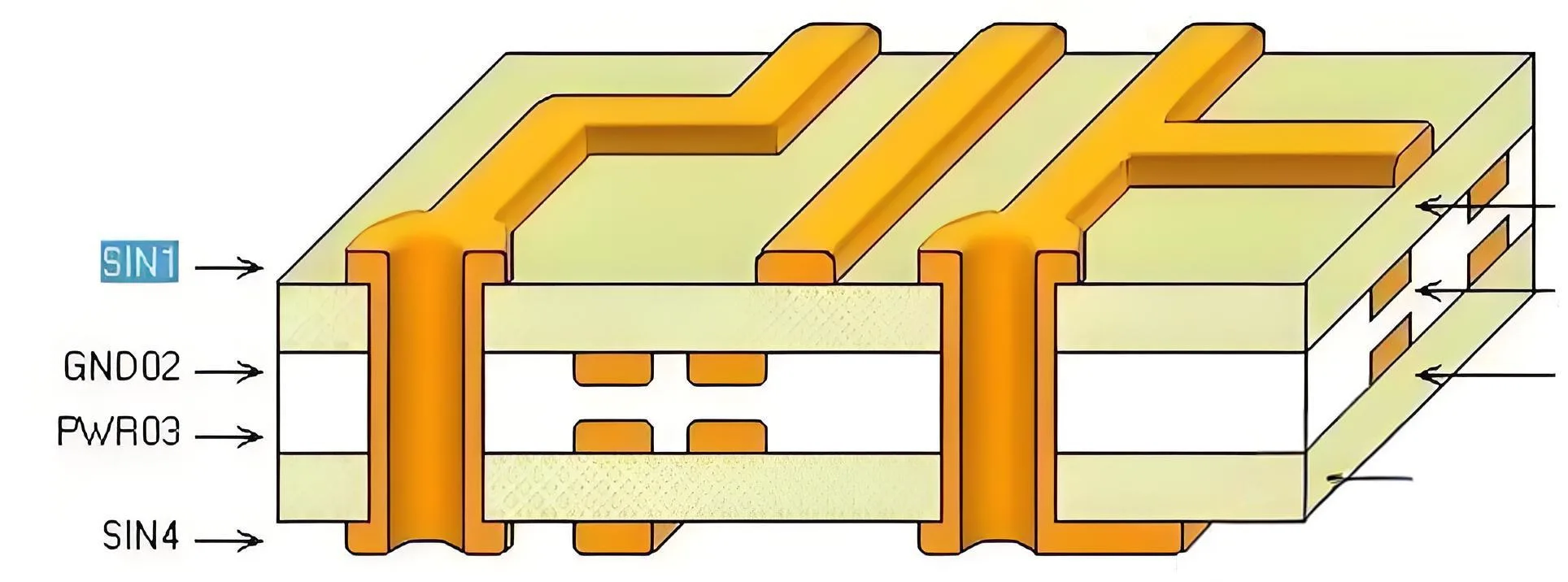

La nostra soluzione di controllo industriale a 4 livelli:
L1 (Signal) - Prepreg - L2(GND Plane) - Core - L3(PWR Plane) - Prepreg - L4(Signal)
Usi Isola FR408HR (εᵣ=3,75, Tg=180°C) con 13 anni di esperienza nel database dei materiali, raggiungimento della tangente di perdita di 0.009 (@10GHz).
Principi di routing intelligente orientati al DFM
-
Segnali ad alta velocità: Tolleranza di corrispondenza della lunghezza ≤50mil
-
Instradamento della potenza: 20Regola H (inserto piano di potenza ≥20×spessore dielettrico)
-
Standard DFM: 4/4mil traccia/spazio, ≥8mil trapani (compatibile con 20 produttori globali di PCBA)
Soluzioni di ingegneria termica
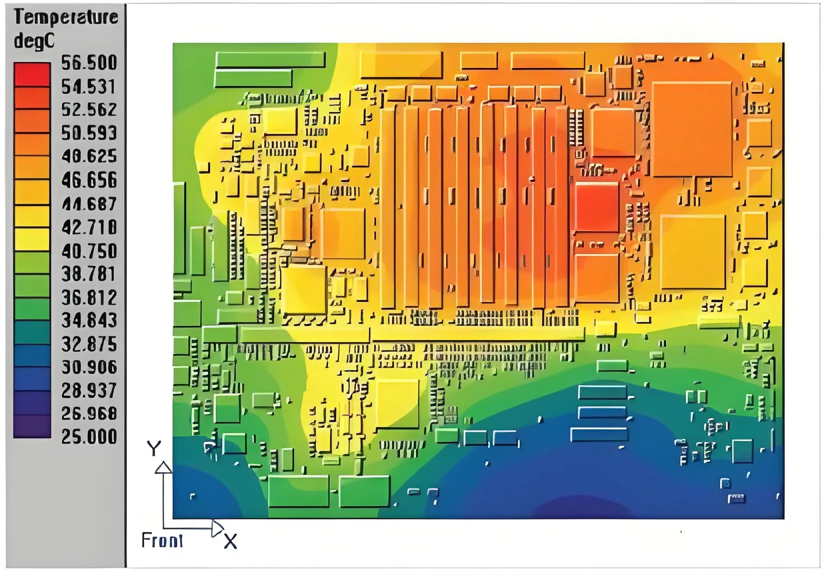

Analisi termica per servoazionamento da 200 W:
-
Nessun raffreddamento: Temperatura giunzione IC 148°C (Critico)
-
Con via termica 4×24: 107° C.
-
Con rame localizzato da 2 once: 92° C. (Raggio d'azione sicuro)
Sistema di verifica della progettazione PCB end-to-end
• DFA schematico → Verifica dell'assieme 3D → Simulazione SI/PI → Analisi dello stress termico → Rapporto DFM
Storie di successo dei clienti: Competenza tecnica che guida il valore aziendale
Innovazione nella progettazione di gateway IoT industriali
-
Sfida: 6-scheda a strati con 5xGbE + WiFi6 (EMI 23 dB oltre il limite)
-
Soluzioni:
✓ Instradamento pseudo-differenziale (spaziatura=2×larghezza)
✓ Segmentazione del piano di potenza a scacchiera
✓ Messa a terra della gabbia di Faraday IC -
Risultato: Certificazione FCC superata, 99.2% resa produttiva
Ottimizzazione della scheda EV BMS
-
Parametri: 12-PCB in rame pesante a strati, 300Una corrente continua
-
Innovazioni:
✓ Blocchi di rame incastonati da 400μm
✓ 17% riduzione dei costi dei dissipatori di calore attraverso la simulazione termica
✓ 22% riduzione dimensionale con microvie HDI -
Impatto: Ordine automobilistico assicurato di 100.000 unità
Perché i clienti globali scelgono i servizi di progettazione PCB di UGPCB
Vantaggi dell'ecosistema tecnologico
-
Progettazione basata sui dati: Database dei materiali con <3% errore (78 substrati, 256 combinazioni di lamine)
-
Piattaforma collaborativa: Supporto nativo di file Allegro/PADS/Altium
-
Motore della conoscenza: 37 norme integrate (IPC-2221/2152 ecc.)
Efficienza del servizio a ciclo completo

Vantaggi quantificabili per il cliente
-
Riduzione dei costi: 18% riduzione della dimensione media della scheda attraverso l'ottimizzazione DFM
-
Efficienza: 92% percentuale di successo al primo passaggio (37% superiore alla media del settore)
-
Mitigazione del rischio: 85%+ Problemi EMI/SI risolti in pre-produzione
Inizia il tuo percorso di progettazione PCB ad alta affidabilità
Quando un cliente automobilistico tedesco ha dovuto affrontare guasti al bus CAN che hanno ritardato la produzione, UGPCB ha risolto i problemi in 48 ore attraverso ristrutturazione del piano di riferimento E corrispondenza della terminazione – proving our “Design-for-Manufacturing” philosophy where every 0.1mm trace optimization impacts market success.
Ottieni supporto per la progettazione PCB personalizzata oggi stesso:
① Programma 1-on-1 Consultazione con gli ingegneri senior
② Supporto tecnico professionale gratuito