


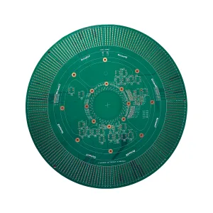
Introduction to UGPCB’s ATE Probe Card PCB
UGPCB’s 50-layer ATE (Attrezzatura di prova automatizzata) Probe Card PCB is a precision-engineered solution designed for high-frequency semiconductor testing. It enables accurate signal transmission between test equipment and integrated circuits (ICS), ensuring reliable performance in mission-critical environments.

Key Technical Specifications
-
Conta dei strati: 50 strati
-
Spessore: 198 mil
-
Materiale: Fr4 htg (High-Temperature Glass Epoxy)
-
Dimensione minima del foro: 5 mil
-
Spaziatura BGA: 0.35mm
- Spessore del rame:2/2oz
-
Proporzioni: 40:1
-
Distanza trapano-rame: 3 mil
-
Pofv (Placcato sopra riempito Via): SÌ
-
Finitura superficiale: Eneg (Electroless Nickel Electroless Gold)
Design and Structural Innovations
Critical Design Features
-
High-Density Interconnects: The 50-layer architecture supports ultra-fine routing for BGA components with a 0.35mm pitch, essential for modern IC testing.
-
Advanced Material: FR4 HTg ensures thermal stability (Tg ≥ 180°C), preventing deformation during high-power testing cycles.
-
Foratura di precisione: UN 40:1 aspect ratio and 5 mil microvias enable reliable signal paths in tightly spaced layouts.
-
Tecnologia POFV: Filled and plated vias enhance mechanical strength and thermal dissipation, critical for prolonged testing operations.
Structural Advantages
-
Ultra-Short Drill-to-Copper Distance: 3 mil spacing minimizes signal loss and crosstalk.
-
ENEG Surface Finish: Provides exceptional oxidation resistance and stable contact surfaces for probe needles.
Performance and Functional Applications
Principi operativi
The PCB routes electrical signals between test probes and ICs with minimal latency. The FR4 HTg substrate maintains dielectric consistency under thermal stress, while POFV ensures uninterrupted connectivity in high-vibration environments.
Metriche chiave delle prestazioni
-
Thermal Endurance: Stable performance at temperatures up to 180°C.
-
Integrità del segnale: Controlled impedance (±8%) and low insertion loss (<0.5db).
-
Mechanical Durability: Resists delamination during 10,000+ test cycles.
Casi d'uso primari
-
Test dei semiconduttori: Validates logic chips, moduli di memoria, and processors in ATE systems.
-
Aerospace Electronics: Used in avionics testing rigs requiring ultra-reliable PCBs.
-
5G and IoT Device Production: Ensures signal accuracy in high-frequency RF component testing.
-
Automotive IC Validation: Deployed in ADAS and ECU testing workflows.
Processo produttivo e garanzia della qualità
Flusso di lavoro manifatturiero
-
Material Cutting: FR4 HTg laminates are precision-cut to required dimensions.
-
Perforazione laser: Raggiunge 5 mil holes with a 40:1 aspect ratio using CO₂ lasers.
-
Plating and Via Filling: POFV technology reinforces vias with copper plating.
-
Allineamento dei livelli: 50-layer stackup is bonded under high pressure and temperature.
-
Trattamento superficiale: ENEG coating is applied for corrosion resistance.
-
Rigorous Testing: Includes electrical continuity checks, impedance testing, and thermal cycling validation.
Quality Standards
-
Classe IPC-6012 3 Conformità: Guarantees reliability for harsh industrial applications.
-
100% Ispezione ottica automatizzata (AOI): Detects micro-defects in high-density layouts.
Summary of Competitive Advantages
-
Ultra-High Density: Supports miniaturized IC testing with 0.35mm BGA spacing.
-
Resilienza termica: FR4 HTg ensures stability in extreme conditions.
-
Industry-Leading Precision: 5 mil microvias and 3 mil drill-to-copper spacing.
-
Broad Compatibility: Compatible with major ATE platforms like Teradyne and Advantest.
This PCB combines cutting-edge engineering, stringent quality controls, and specialized materials to meet the demands of next-generation semiconductor testing.