


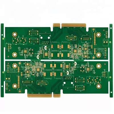
Overview of 6 Layer Golden Finger PCB
IL 6 Layer Golden Finger PCB is a high-precision, multi-layered printed circuit board designed for advanced electronic applications. This product combines multiple layers of conductive traces and insulating materials to provide exceptional performance and reliability in various electronic devices.
Definizione
UN 6 Layer Golden Finger PCB is a type of multi-layer printed circuit board (PCB) that features six individual layers of conductive material, separati da strati isolanti. The term “Golden Finger” refers to the specific surface treatment applied to the edges of the board, which involves immersion gold and additional gold plating on the contact fingers.
Requisiti di progettazione
When designing a 6 Layer Golden Finger PCB, several key requirements must be considered:
- Qualità del materiale: High-quality FR4 material is essential for durability and performance.
- Configurazione del livello: Six layers are needed to accommodate complex circuitry and signal routing.
- Spessore del rame: A standard copper thickness of 1OZ ensures adequate conductivity.
- Trattamento superficiale: Immersion gold with additional gold finger plating enhances connectivity and corrosion resistance.
- Dimensioni di traccia/spazio: A minimum trace/space of 4mil/4mil is required for precise circuit patterns.
- Processi speciali: The gold finger process with a thickness of 0.1um is critical for reliable edge connections.
Principio di lavoro
IL 6 Layer Golden Finger PCB operates based on the principles of electrical conductivity and insulation. Conductive traces on different layers create pathways for electrical signals, mentre gli strati isolanti impediscono interazioni indesiderate tra questi segnali. The gold finger edges facilitate easy insertion into connectors, ensuring stable and reliable connections.
Applicazioni
This type of PCB is widely used in applications that require high precision and reliability, ad esempio:
- High-speed digital circuits
- Attrezzatura di telecomunicazioni
- Advanced computing systems
- Elettronica automobilistica
- Medical devices
Classificazione
6 Layer Golden Finger PCBs can be classified based on their intended use, ad esempio:
- Schede di elaborazione del segnale: Per gestire segnali ad alta frequenza nei dispositivi di comunicazione.
- Schede di distribuzione dell'energia: Gestire l'alimentazione in sistemi elettronici complessi.
- Schede di controllo: For controlling and managing various functions in electronic devices.
Materiali
The primary materials used in the construction of a 6 Layer Golden Finger PCB include:
- Materiale di base: FR4, Un materiale in fibra di vetro retardante di fiamma noto per le sue eccellenti proprietà dielettriche e la resistenza meccanica.
- Materiale conduttivo: Rame, Utilizzato per le tracce conduttive.
- Trattamento superficiale: Immersion gold and additional gold plating for the gold fingers.
Prestazione
Le prestazioni di a 6 Layer Golden Finger PCB is characterized by:
- Alta integrità del segnale: A causa delle dimensioni di traccia/spazio precise e materiali di qualità.
- Connettività affidabile: Ensured by the gold finger surface treatment.
- Durata: Enhanced by the robust FR4 base material and immersion gold finish.
- Efficienza elettrica: Perdita del segnale ridotta al minimo e interferenza dovuta alla configurazione del livello ottimizzato.
Struttura
The structure of a 6 Layer Golden Finger PCB consists of:
- Sei strati di materiale conduttivo: Alternando gli strati isolanti.
- Gold Finger Edges: Plated with a thin layer of gold for enhanced connectivity.
- Protective Layers: Including solder mask and silkscreen for protection and identification.
Caratteristiche
Key features of the 6 Layer Golden Finger PCB include:
- Trattamento superficiale avanzato: Immersion gold plus gold finger for superior connection quality.
- Alta precisione: With a minimum trace/space of 4mil/4mil.
- Opzioni di colore personalizzabili: Disponibile in verde o bianco.
- Spessore standard: With a finished thickness of 1.6mm.
Processo di produzione
The production process for a 6 Layer Golden Finger PCB involves several steps:
- Preparazione del materiale: Selezione e preparazione di fogli FR4 e foglio di rame.
- Stacking strato: Strati alternati di rame e materiali isolanti.
- Incisione: Rimozione del rame in eccesso per formare il modello di circuito desiderato.
- Placcatura: Applying immersion gold and additional gold finger plating.
- Laminazione: Combinando gli strati sotto calore e pressione.
- Perforazione: Creazione di buchi per componenti a foro e Vias.
- Applicazione della maschera di saldatura: Protezione del circuito da ponti di saldatura e fattori ambientali.
- Silkscreen Printing: Aggiunta di testo e simboli per il posizionamento e l'identificazione dei componenti.
- Controllo di qualità: Garantire che il PCB soddisfi tutte le specifiche e gli standard di progettazione.
Usa gli scenari
IL 6 Layer Golden Finger PCB is ideal for scenarios where:
- L'elevata integrità del segnale è cruciale.
- Sono richieste connessioni affidabili e durevoli.
- I vincoli di spazio richiedono un design compatto ed efficiente.
- È necessario un trattamento avanzato di superficie per prestazioni migliorate.