Pushing Boundaries: How HDI PCB Design Capabilities Reshape the Micro-World of Electronics
On the battlefield of high-density interconnects, a 0.035mm trace width represents engineers conversing with the laws of physics, while each precisely crafted layer stack redefines the microscopic realm.
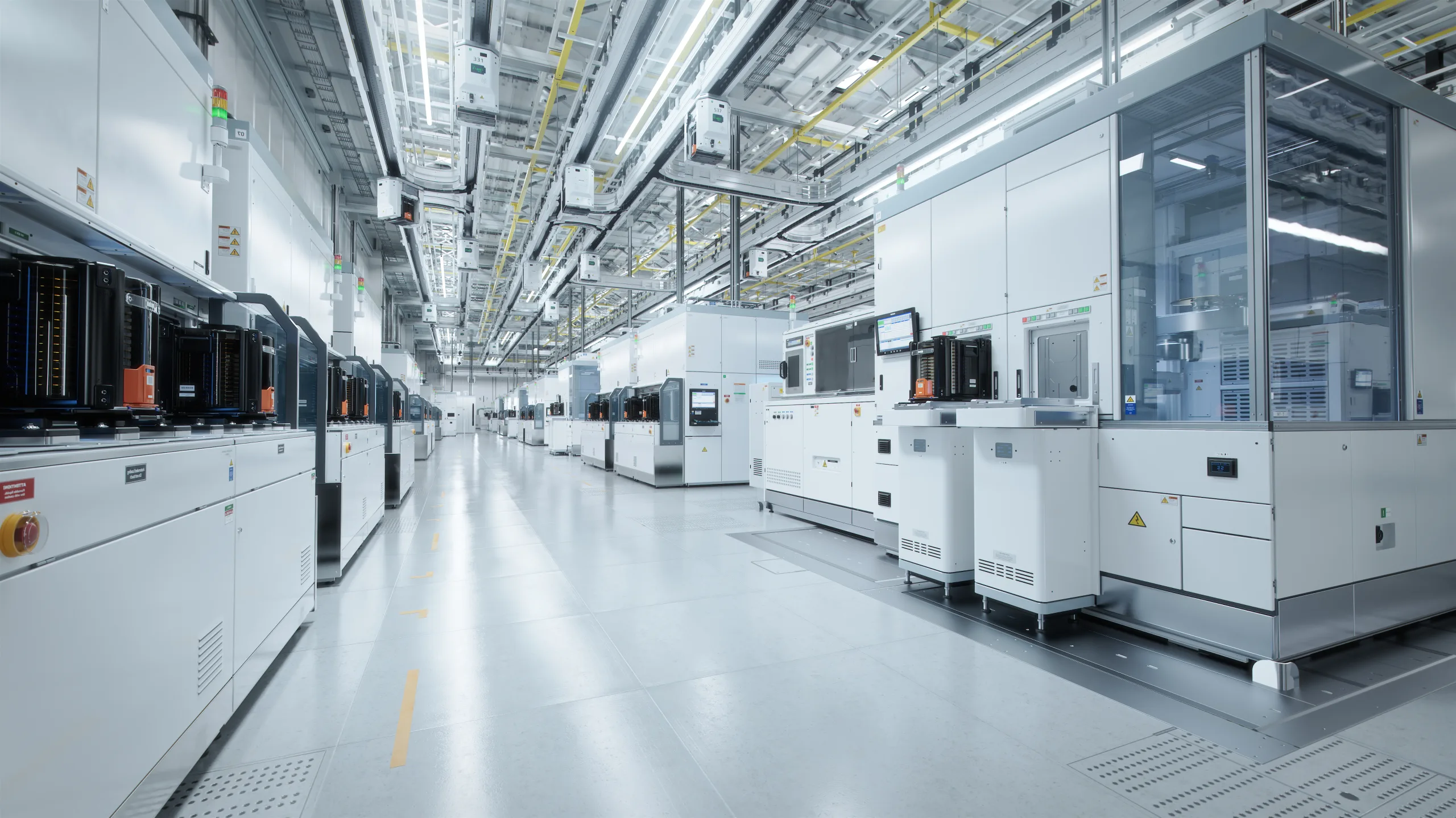
Smartphones flip effortlessly in your palm, 5G signals traverse the air silently, medical devices probe the body with pinpoint accuracy – the core engines of these modern marvels reside within an HDI PCB often no larger than a fingernail. When circuit density exceeds 120 inches per square inch, 伝統的 プリント基板 technology falters, making high-density interconnect (HDI) technology the essential key.
HDI PCB: Defining the Miniaturization Revolution in Electronics
HDI PCB (High-Density Interconnect Printed Circuit Boards) achieve wiring densities far exceeding 従来のPCB through revolutionary micro-via technology. Its core lies in:
-
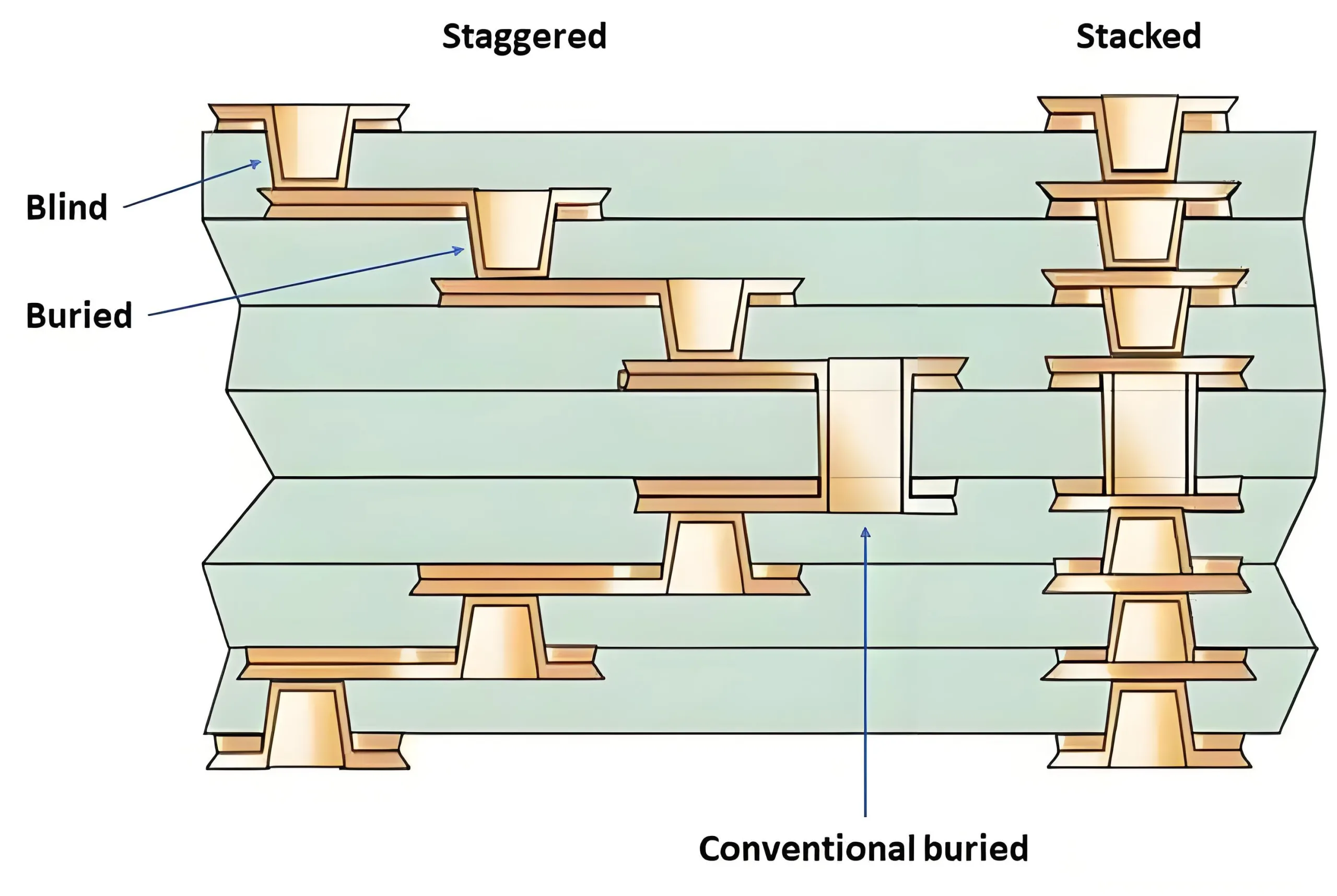
Ultra-Micro Via Structures: Utilizing 0.2mm buried vias and 0.1-0.05mm laser-drilled blind vias for layer interconnection.
-
Stackup Hierarchy Definition: Each additional layer of laser-drilled blind vias increases the HDI tier (例えば。, 1+n+1, 2+n+2).
-
Any-Layer HDI Architecture: Eliminates buried vias, relying entirely on laser-drilled blind vias for unrestricted interconnection between any layers.
Blind Via Process: The Battlefield of Micron-Level Precision
When PCB designers sketch at the bleeding edge of 0.05mm trace widths, manufacturing processes face a triple challenge:
The Process Divide: Stacked vs. Non-Stacked Via Designs
-
Non-Stacked Via Design: Inner layer imaging → Lamination → Browning → Laser Drilling → De-browning → Electroless Copper → Panel Plating…
-
Stacked Via Design: Inner layer imaging → Lamination → Browning → Laser Drilling → De-browning → Electroless Copper → Panel Via Filling Plating → Copper Thinning…
The critical difference: Stacked blind vias must be completely filled, otherwise lamination risks catastrophic delamination (“blowout”). UGPCB employs advanced electroplating via fill technology, 達成 >98% intra-via copper density, significantly exceeding IPC-6012E standards.
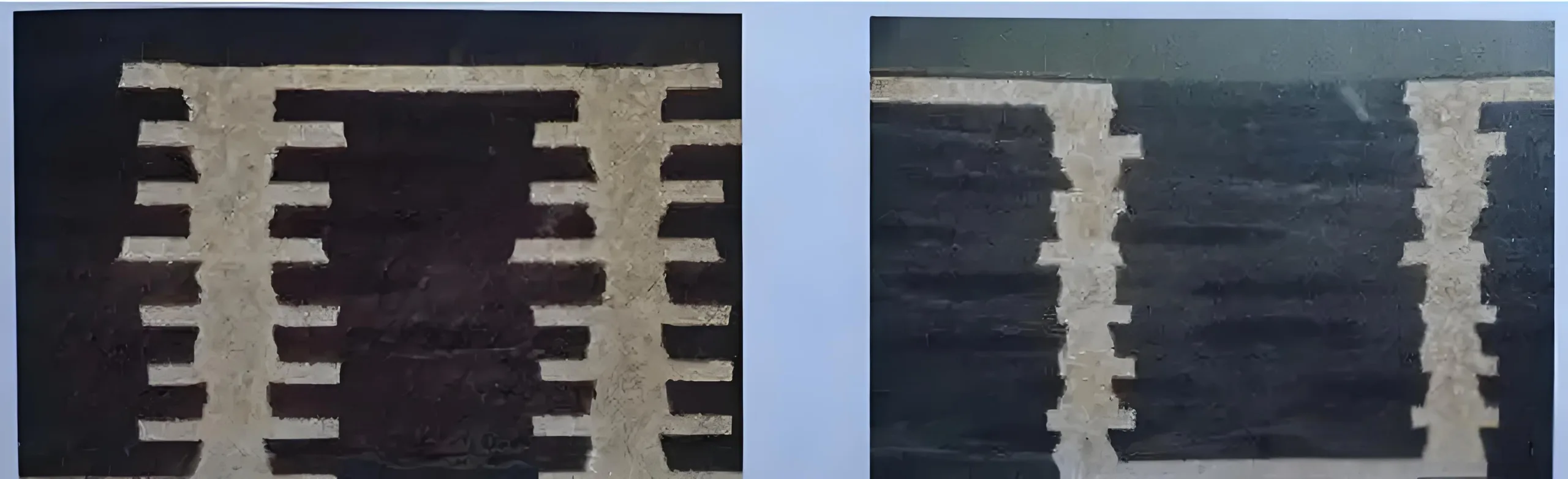
The Contenders in Via Fill Technology
Resin Plugging vs. Electroplated Copper Filling Performance Comparison:
| パラメーター | Resin Plugging | Electroplated Copper Fill |
|---|---|---|
| 熱信頼性 | Prone to cracking (ΔTg >150℃) | Withstands 300°C thermal shock |
| 導電率 | Surface copper layer only | Solid copper conduction |
| Surface Flatness | ≤15μm depression | ≤5μm ultra-flat |
| コスト効率 | Lower (3 ステップ) | Higher (requires precision control) |
Electroplated copper filling, with its superior conductivity and reliability, is the preferred solution for high-end HDI PCB manufacturing.
HDI Manufacturing Capability: The Technical Supremacy Behind the Numbers
UGPCB’s production line data reveals industry-leading capabilities:
Manufacturing Capability Formula:
Minimum Trace/Space = k * (Laser Precision + Registration Capability)
Where k ≈ 0.7 (Process Capability Coefficient)
-
Layer Breakthrough: 量産: 24 レイヤー; プロトタイプ: 36 レイヤー (stackup tolerance ±3%)
-
Trace/Space Limit: 量産: 2ミル/2ミル (0.05mm); プロトタイプ: 1.5千/1.5mil (0.035mm)
-
Micro-Via Precision: Laser drill positional accuracy ±15μm; Via diameter tolerance ±10μm
Five Golden Rules for Selecting an HDI Supplier
When sourcing high-reliability HDI PCBs, rigorously verify your supplier’s:
-
Stacked Via Process Certification: IPC-2226 Class III compliance.
-
Material Library Depth: Stock availability of 高速材料 like M7NE, EM-827.
-
Inspection Precision: AOI equipment resolution ≤10μm; AXI inspection capability.
-
Yield Control: Mass production yield ≥95% for 8-layer, 1+N+1 HDI.
-
Technical Responsiveness: 24-hour engineering support response.
ケーススタディ: A medical device manufacturer experienced a 37% surge in failure rates during accelerated aging tests for an implantable heart monitor due to selecting a supplier lacking electroplated fill capability for stacked vias. Switching to UGPCB’s Any-Layer HDI solution reduced device volume by 40% and increased MTBF (Mean Time Between Failures) に 50,000 時間.
今行動してください: Unlock Your HDI Innovation Potential
Is your PCB design facing:
-
Routing challenges with chip pin pitches ≤0.4mm?
-
Signal integrity hurdles for 10Gbps+ high-speed designs?
-
Space compression demands in wearable devices?
Professional HDI PCB solutions are your key to breakthrough success.
Get Your Custom HDI PCB Quote Today!
Our engineering team is ready to:
→ Analyze your design files for stackup optimization opportunities.
→ Develop a process roadmap achieving up to 15% コスト削減.
Connect with HDI PCB Design Experts Online and receive a professional DFM report with an accurate quote within 2 時間.
微信
WeChat で QR コードをスキャンします