
アナログの領域で 回路設計, 運用アンプ, 精密抵抗器, そして、コンデンサはしばしばスポットライトを主張します. しかし、システムパフォーマンスの制限の真の決定要因は、舞台裏で働く隠された首謀者です: の プリント基板 (プリント基板). このサイレントファンデーションは、統治中にすべてのコンポーネントを搭載しています 信号の完全性, ノイズ抑制, そして システムの信頼性 トレースのすべてのミリメートルを通して, 各誘電層, そして、すべての接地決定.
PCB材料科学: FR評価を超えて高周波性能を解読します
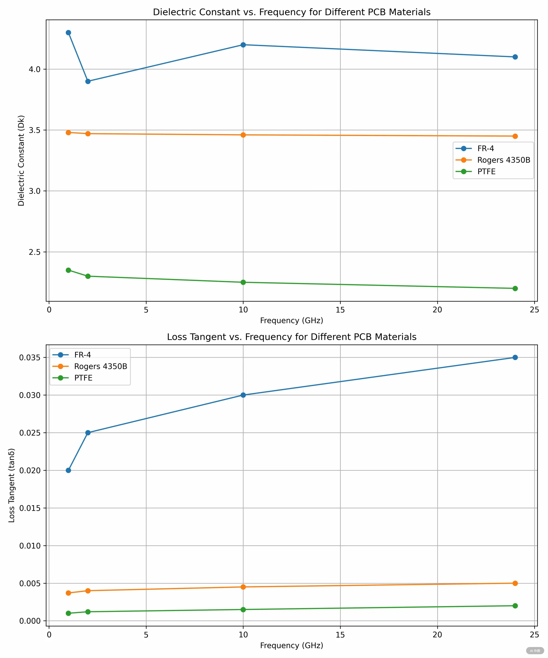
議論するとき プリント基板材料, FR-4の可燃性評価は、単なるプロローグです. 高速アナログ回路用, 誘電率 (DK) そして 損失係数 (タンδ) 目に見えないハンドシグナルシグナルの運命です.
信号伝播速度 (v) によって決定されます:
v = c / √(ε_r)
ここで、 * c * =光の速度, E_R =相対誘電率. FR-4のε_Rは間に変動します 4.2-4.8, 原因 5% 信号遅延変動. もっと批判的です, その損失特性 - 10GHzで, 標準のFR-4は、tanδ= 0.02を示します, と同等 0.5インチあたりのDB信号損失.
湿度温度相互作用 精度の回路で特に致命的であることが証明されています:
-
1% 水分吸収により、FR-4表面抵抗が3桁減少します
-
15% 85°Cシフトフィルター中心周波数を壊滅的にシフトするDKドリフト
専門家の洞察: Rogers 4350bを使用した医療PCB (E_R = 3.48±0.05) 維持する <2% -40°Cから +150°CへのDK変動 - 生命維持監視機器にとって重要.
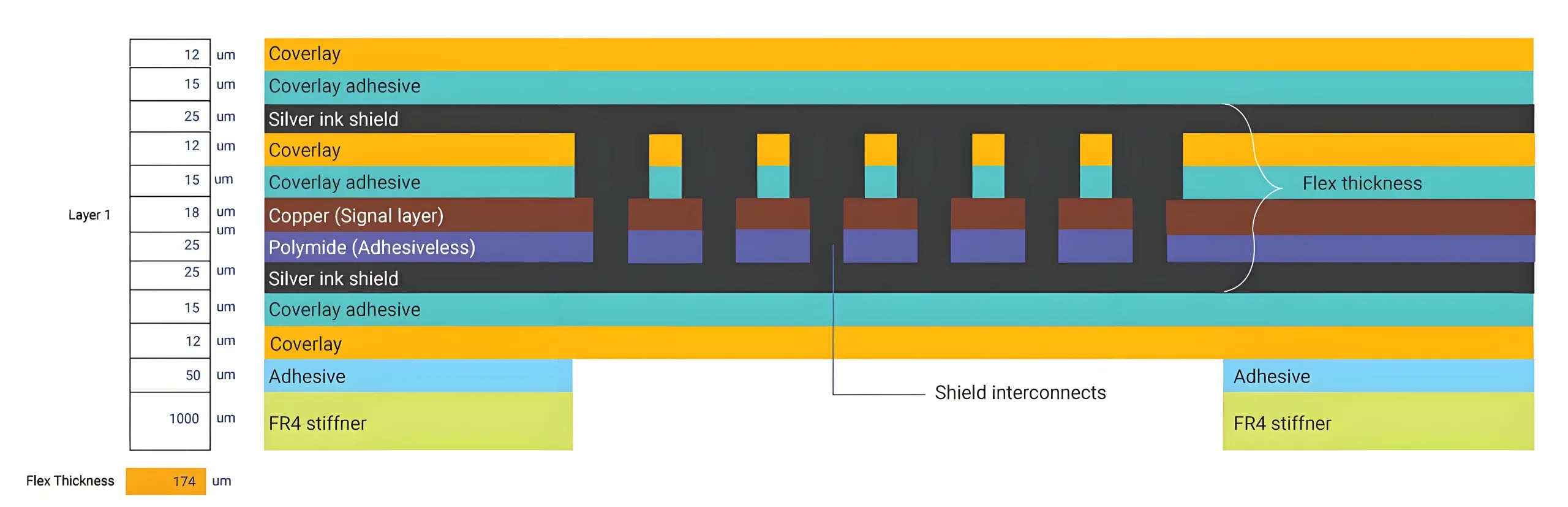
PCBスタックアップアーキテクチャ: エンジニアリング現在のパス & EMIシールド
単一/二重層の制限
10MHzシグナルを超えて, 1.6MM両面ボードは、接地層の弱点を明らかにします. 層間容量:
C = (ε_0 * ε_r * A) / d
標準の1.6mmボードは、35pf/in²のみを達成します >100MHzノイズ抑制.
4層スタックアップ革命
専用の電力/地上飛行機はインピーダンス制御を変換します:
-
0.2MM誘電体は280pf/IN²に容量を高めます
-
グランドプレーン抵抗は、単一層の1/100に低下します
-
放射ノイズの減衰は40dB増加します
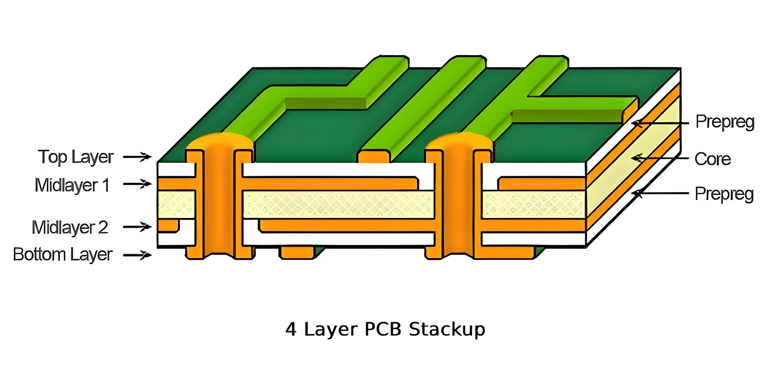 検証データ: UGPCB ラボテストでは、4層の設計が78μVPPから12μVPPにオペアンプの出力ノイズを減らすことを示しています - 85% 改善.
接地戦略: アナログデジタル境界の確立
平面分離の臨界
重複するデジタル/アナログの地上飛行機は、容量性ノイズチャネルを作成します:
C_coupling = (ε * A_overlap) / d
1.6mmボードの0.1mm²のオーバーラップでも、0.3pfの結合容量を生成します。100MHzクロックノイズをμVレベルのアナログ信号に注入するのに十分です。.
星の接地原理
単一点接地は、数学的に接地ループを排除します:
V_noise = -dΦ/dt = -2πf * B * A
どこ B =磁束密度, あ =ループ領域. ある時点での収束パスは、ループ領域を最小限に抑えます.
コンポーネント周波数マスキング: 抵抗器がインダクタになるとき
抵抗性寄生虫
0805 フィルム抵抗器には、約2NHの寄生インダクタンスが含まれています. 100MHzで:
X_L = 2πfL = 1.26Ω
典型的な抵抗値を超えます, 回路の動作を根本的に変更します.
容量性自己共感トラップ
コンデンサのインピーダンスが続きます:
|Z| = √[R_ESR² + (X_L - X_C)²]
標準の10μFタンタルコンデンサは、300kHzで自己共同です, 10MHzで0.1μFセラミックによってアウトパフォームされています:
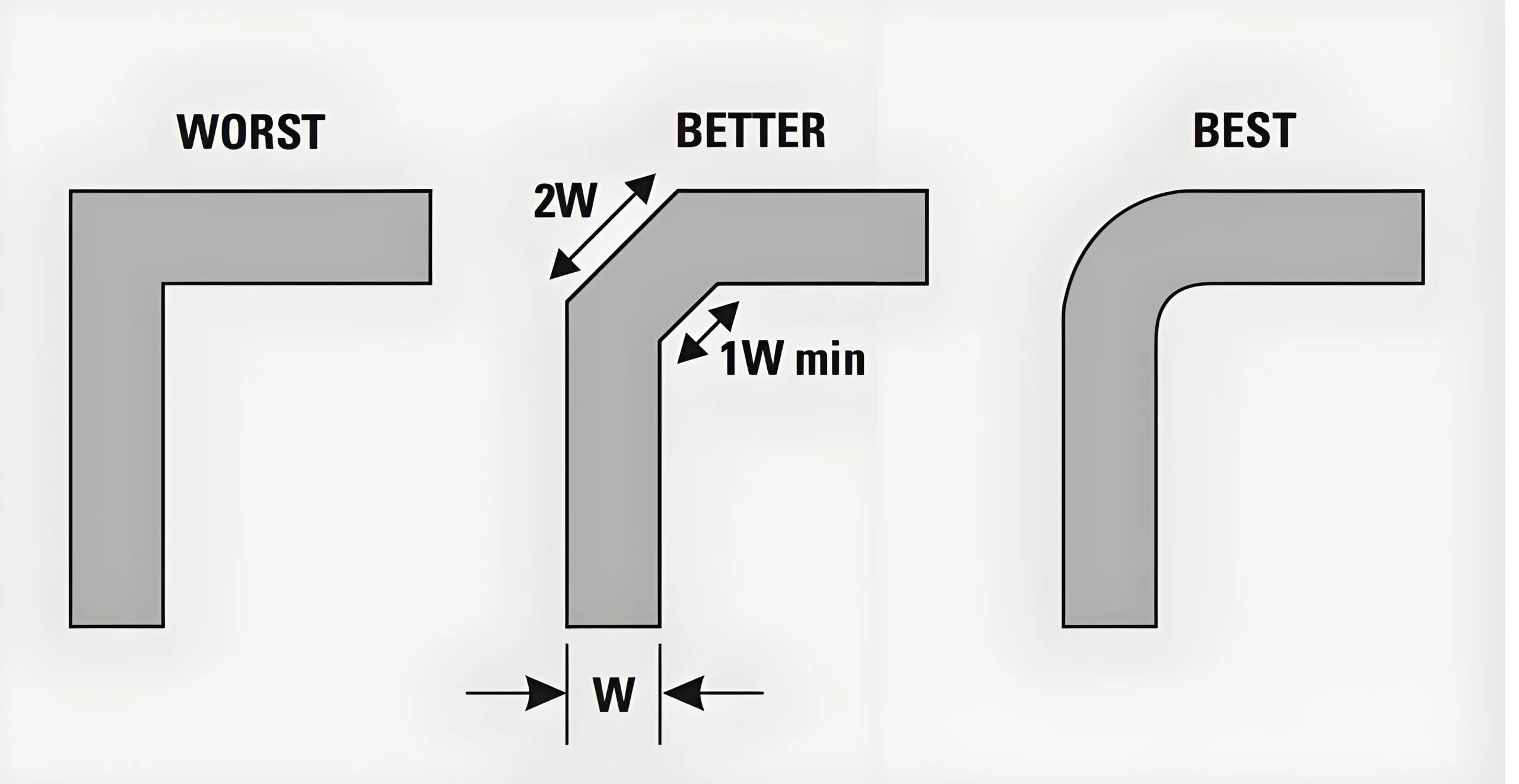
ルーティングジオメトリ: 90°曲げのem catastrophe
右角痕跡は、高速で隠されたアンテナとして機能します PCBレイアウト:
-
トレースの長さを効果的に増やします 26%
-
コーナー容量は、インピーダンスの不連続性を引き起こします
-
45°の曲げよりも効率的に30dBを放射します
Viasは等しい危険性を示します. 0.3mm Viaの寄生インダクタンス:
L ≈ 5.08h [ln(4h/d) + 1] (pH)
ここで、 * h * =ボードの厚さ (mm), *d* =穴の直径 (mm). 1GHzで, 1.6mmのシングルボードは1.6Ωのリアクタンスを生成します.
究極の防御: ナノクリーニングからファラデーエンクロージャーまで
イオン汚染制御
高インピーダンスノードには、以下のイオン残基が必要です:
<1.56 μg/cm² (IPC J-STD-001 Class 3)
DI水による超音波洗浄は達成されます <0.3μg/cm².
EMIシールド効果
ファラデーケージのパフォーマンスが続きます:
SE(dB) = 20log[(Z_0)/(4Z_s)] + 20log(e^(t/δ))
どこ d =肌の深さ. 1MMアルミニウムは、1GHzで120dB減衰を提供します, しかし、0.1mmのギャップはこれを30dBに分解します.
目に見えない建築家の啓示
データは驚くべき真実を明らかにします: 68%+ 回路の障害は、PCB設計上の欠陥に由来します. かつては単なるコンポーネントキャリアと見なされます, PCBは実際には ミッションクリティカルなシステムアーキテクト.
10GHz回路で:
-
FR-4誘電損失は、15dBの信号エネルギーを消費する可能性があります
-
0.5MMグラウンドジャンプは300mVのグラウンドバウンスを誘導します
-
顕微鏡フラックス残基は漏れ経路を作り出します
設計革命は、パラダイムシフトから始まります: コストアイテムからPCBを再分類します コア機能要素. 次のオペアンプをレイアウトするとき:
-
その0.1Bノイズの改善は、ラミネートDK値に存在します
-
これらの3PSタイミングマージンは、地上の平面厚に存在します
これを高めます “目に見えないアーキテクト” バックステージからセンターステージまで, アナログサーキットはパフォーマンスの障壁を打ち破ります.
