
導入: DDR5 PCB設計におけるミリメートルスケールの戦争
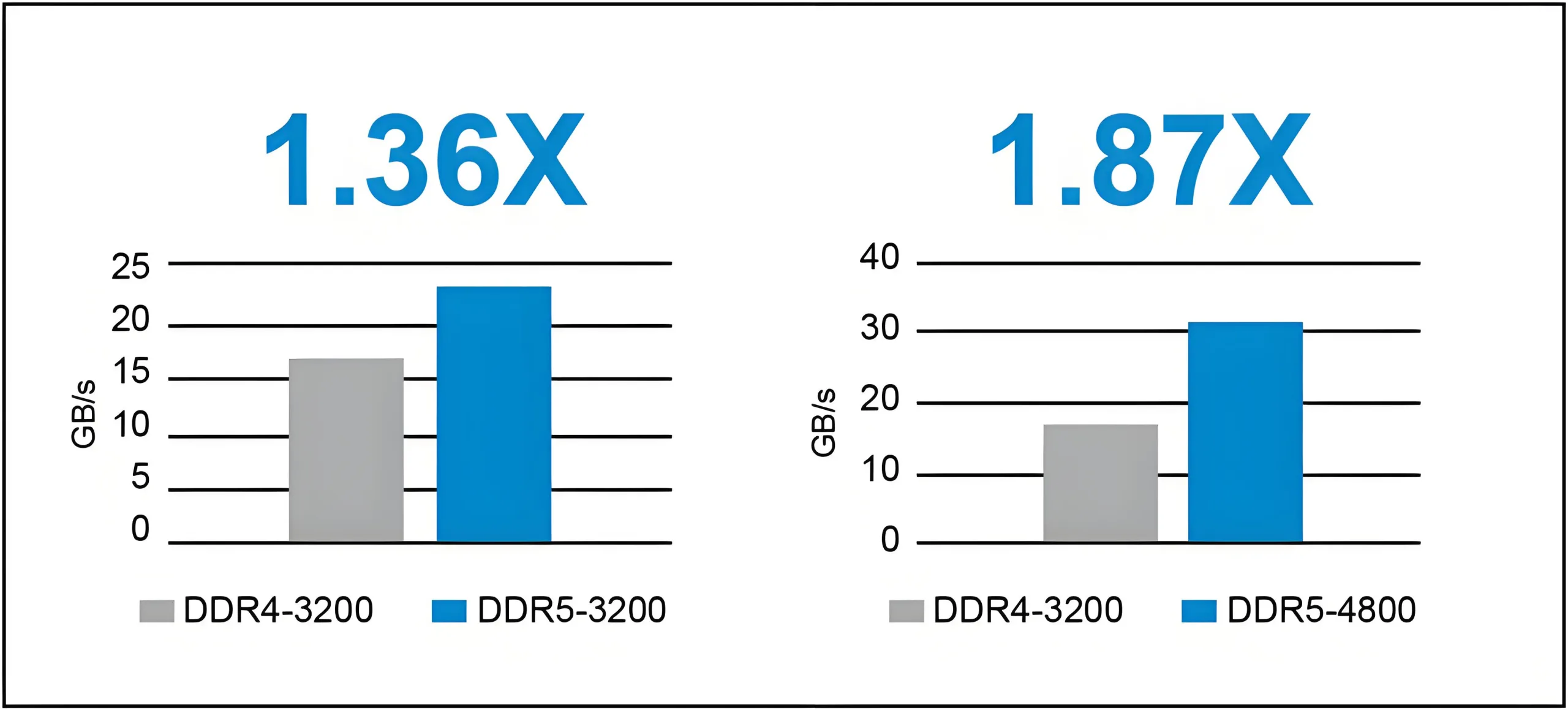
DDR4からDDR5への跳躍は、パラダイムシフトをマークします: 信号速度が急増します 3,200 mt/s to 6,400 動作中のMT/sは、1.1Vに急落します. この二重の挑戦は変革します プリント基板 シンプルな接続エンジニアリングからミリメートルスケールの精密戦争へのルーティング. 業界のデータはそれを明らかにしています 80% DDR5の設計障害の障害は、ルーティングの問題に由来します, と 90% レイアウト前のシミュレーションにより予防可能. この記事では、5つの重要なDDR5ルーティングの落とし穴を分析します, 経験的データとケーススタディによってサポートされています, PCB専門家に実用的なソリューションを提供します.
1. DDR5物理的特性: 従来のPCB設計方法が失敗する理由
1.1 信号速度と帯域幅革命
DDR5-6400の場合, 有効なクロック周波数に到達します 3,200 MHz, エッジレートと同じくらい速い 0.5 詩 (20-80% 立ち上がり時間). これはトリガーします:
-
悪化した皮膚効果: 高周波電流は導体表面に集中します, 効果的な銅の厚さを減らします 0.66 μmで 10 GHz.
-
誘電損失エスカレーション: FR4基板 損失の接線を示します (Df) の 0.02 で 10 GHz, 原因 >3 DB/インチ信号減衰.
式の検証 (肌の深さ):

で F = 10 GHz, Δ≈0.66μm,伝統的な1オンスの銅を残します (35 μm) と <2% 利用.
2. 5つのDDR5ルーティング地雷原と対策
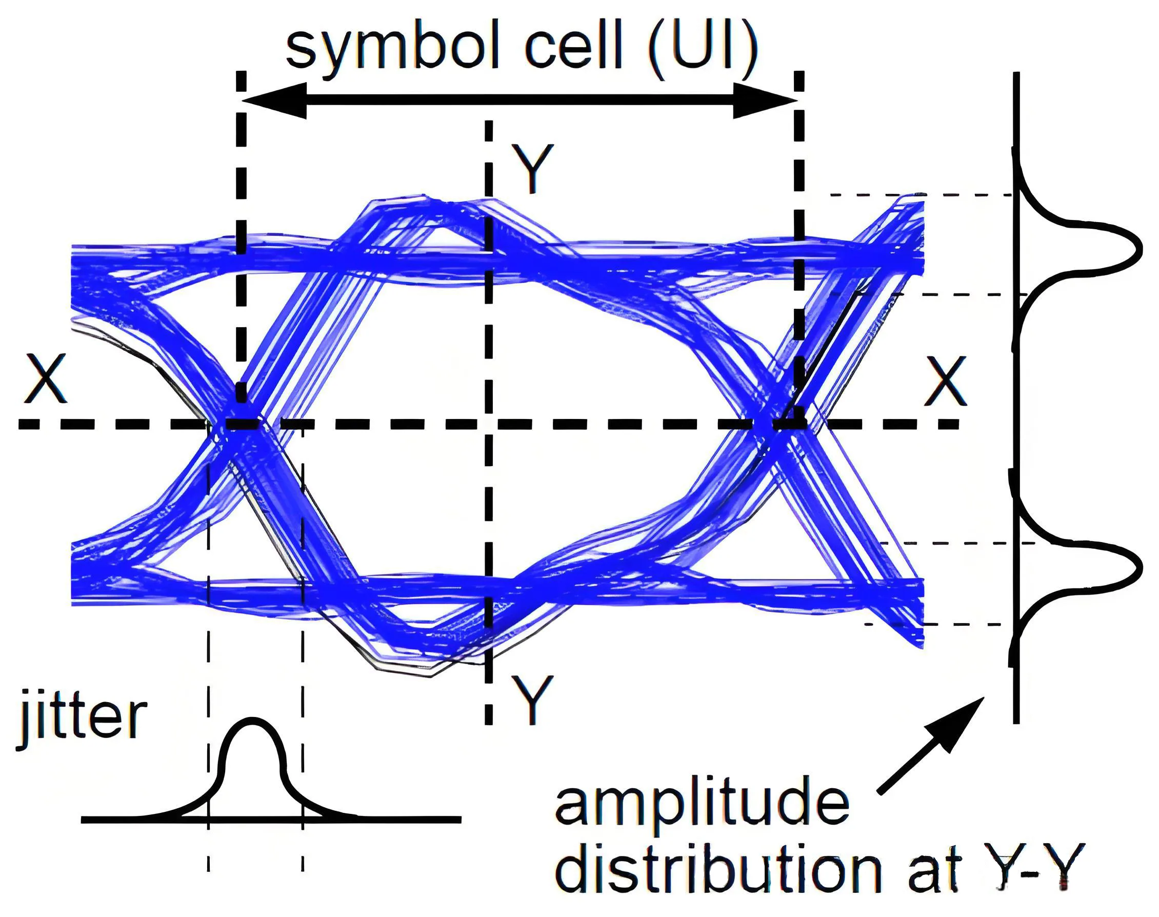
2.1 地雷原 1: タイミングエラー - ±15ps生存しきい値
インパクト: 5milの長さの不一致は±12psの遅延をもたらします, 横の目の幅が崩壊します 30%.
ケーススタディ: GPUの設計は、からのBERの劣化に苦しみました 10-12 に 10-7 8ミルのDQ/DQSスキューによる.
ソリューション:
-
3Dルーティング補償: 90°の蛇行を45°の蛇紋岩に置き換えます, 寄生性容量を減らす 30%.
-
動的タイミングキャリブレーション: モンテカルロシミュレーションを実行します (ケイデンスシグリティ) ±10%のプロセスの変動をカバーします.
式 (タイミングマージン):
Tマージン= tサイクル - - (Tco+Tフライト+Tジッター)
DDR5-6400の場合 (Tサイクル= 0.3125 ), システムアラートトリガーがいつ Tマージン<50 詩.
2.2 地雷原 2: インピーダンスの不連続性 - 5Ω信号津波
リスク: インピーダンスの不一致の原因を介して >15 DBリターンロス, 垂直の目の高さを崩壊させます 40%.
データ: それぞれが追加されていない 0.2 DB挿入損失 @5 GHz.
ソリューション:
-
革命経由: レーザー盲検バイアスを実装します (≤4mil) Antipad補償で, インピーダンスの変動を±3Ωに制限します.
-
パッドの最適化: 楕円パッドを使用します (1.5:1 アスペクト比) 容量性効果を減らすため 20%.
式 (インピーダンスモデルを介して):
zvia≈87ϵr⋅ln(5.98H/(0.8D1+D2))
どこ : 誘電体の厚さ, D1: 直径経由, : パッド径.
2.3 地雷原 3: クロスレイヤー遅延 - 0.1ps/mmバタフライ効果
繊維織り効果: 誘電率の定数変動 (Δϵr = 0.3) ガラス繊維の周期性の原因から 0.6 PS/インチ遅延スキュー.
ソリューション:
-
Z軸アライメント: 0±45°の角度でバイトグループ信号をルートして、誘電体異方性をキャンセルする.
-
クロスレイヤー補償: 自動遅延補正のために、基板DK/DFデータをEDAツールにプリロードする.
2.4 地雷原 4: パワーリップル - 1MV核連鎖反応
感度: 501.1V供給でのMVリップルは、ドライバージッターを増やします 20%.
シミュレーション: PDNターゲットインピーダンスは、従来のデザインよりも2MH支配である必要があります。.
ソリューション:
-
3Dコンデンサマトリックス: 0.1μfを展開します (0402) + 10nf (0201) ICS近くのコンデンサ, カバー 10 KHZ – 2 GHz.
-
マイクロコッパーの柱: BGAの下に直径200μmの柱を埋め込みます, カットループインダクタンス 30%.
2.5 地雷原 5: リターンパスの混乱 - 目に見えないEMI爆弾
EMIリスク: 壊れた参照面は、コモンモードノイズを生成します, EMI制限を超える 10 DB.
ソリューション:
-
グラウンドステッチ: グラウンドバイアスを配置します (≤0.1o) 毎 100 信号層の間のMIL.
-
スプリットプレーンブリッジング: 埋もれたコンデンサを使用します (例えば。, AVX 0402B) パワースプリット全体の10NFカップリング用.
3. DDR5デザインゴールデンルール: 式とツールチェーン
3.1 スタブ制限を介して:DDR5-6400の場合 (F = 3.2 GHz) FR4で: スタブマックス≤14.7mm.

3.2 微分ペアの許容範囲:
と Tui= 0.3125 ns そして vp= 6インチ/: ΔL≤1.9ミル.

3.3 PDNインピーダンスターゲット:
50mVのリップルと10a過渡電流の場合: zターゲット≤5MΩ.

4. PCB設計プロセスリエンジニアリング: 試行錯誤からシミュレーション駆動型まで
4.1 トポロジー計画:
-
HFSSのモデルVIA; アンチパッドの寸法を最適化します.
-
Siwaveを介してスタックアップインピーダンスを抽出します; S-Parameterライブラリを構築します.
4.2 ルーティング実行:
-
アレグロでリアルタイムインピーダンスチェックを有効にします; 自動フラグ違反.
-
グループ内のスキュー2以下でフライバイトポロジを実装します.
4.3 検証:
-
アイダイアグラムテストを実行します (キーサイト広告) 70 mV以上の目の高さ.
-
TDR曲線を測定します; インピーダンスの変動を±5%に制限する.
結論: The “三体” DDR5設計の法則
GHz-Speedの下, マウンドヌック, およびミクロン耐性の制約, DDR5 PCB設計はaに入ります “量子力学” 時代. 信号整合性の戦争における勝利は、材料科学の収束を要求する (低DK基質), 高度なプロセス (msap), およびシミュレーションの習得.
