
電子工学の分野では, のレイヤー数 プリント基板 (プリント基板) 多くの場合、製品の複雑さと技術の洗練度を直接示す指標となります. ほとんどのエンジニアは日常的に次のような作業を行っていますが、 2, 4, or 6-layer boards—with consumer electronics even employing cost-optimized solutions like “pseudo-8-layer” boards (6 機能性電気層プラス 2 断熱層の厚さ)—ハイエンドサーバーの状況は劇的に変化します, ハイパフォーマンスコンピューティングマザーボード, 最先端の通信機器. ここ, プリント基板 16, 32, あるいは 64 レイヤーは共通です. これは重大な疑問を引き起こします: これらを可能にする基本的な設計原則と製造技術は何ですか? 層数の多い PCB? この記事では、技術的な側面を詳細に分析します。, 中核的な課題, 高層数の PCB 向けの高度な製造ソリューション.
高層数の PCB を使用する理由? 単なるルーティング ゲーム以上のもの
PCB 層の数を増やすことは、素晴らしい数字を追求することではありません. 基本的な要因は、現代の電子デバイスのパフォーマンス要求の急激な増加です。. チップのピン密度が上昇し続ける場合 (例えば。, 以上のBGAパッケージ 2500 はんだボール), 信号速度が GHz 領域に入る (例えば。, PCIE 5.0 で 32 GT/秒), システムは同時に高速デジタルを処理する必要があります, RFアナログ, および高出力信号, 伝統的 4 または6層基板では不十分になります.
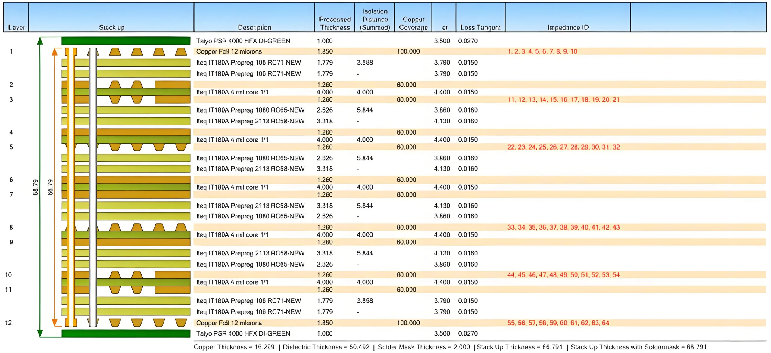
高層数の PCB の中核となる価値は、十分な配線リソースと完全なリファレンス プレーンを提供することにあります。. 一般的な 12 層ボードのスタックアップは次のようになります。: 信号 1 / 地面 / 信号 2 / 力 1 / 信号 3 / 地面 / 信号 4 / 力 2 / 信号 5 / 地面 / 信号 6. This symmetrical “ground-signal-power-signal-ground” stack-up (IPC-2141Aなどのガイドラインに従ってください) インピーダンスを効果的に制御し、高速信号に低ノイズのリターンパスを提供します。. 統計によると、データセンターのスイッチなどの機器では, PCB を使用した設計 20+ レイヤーは、重要なネットワーク信号のクロストークを、 60% (データは IPC TR-579 レポートから参照).

多層基板の設計上の課題: Beyond “Drawing Traces”
シグナルインテグリティとインピーダンス制御
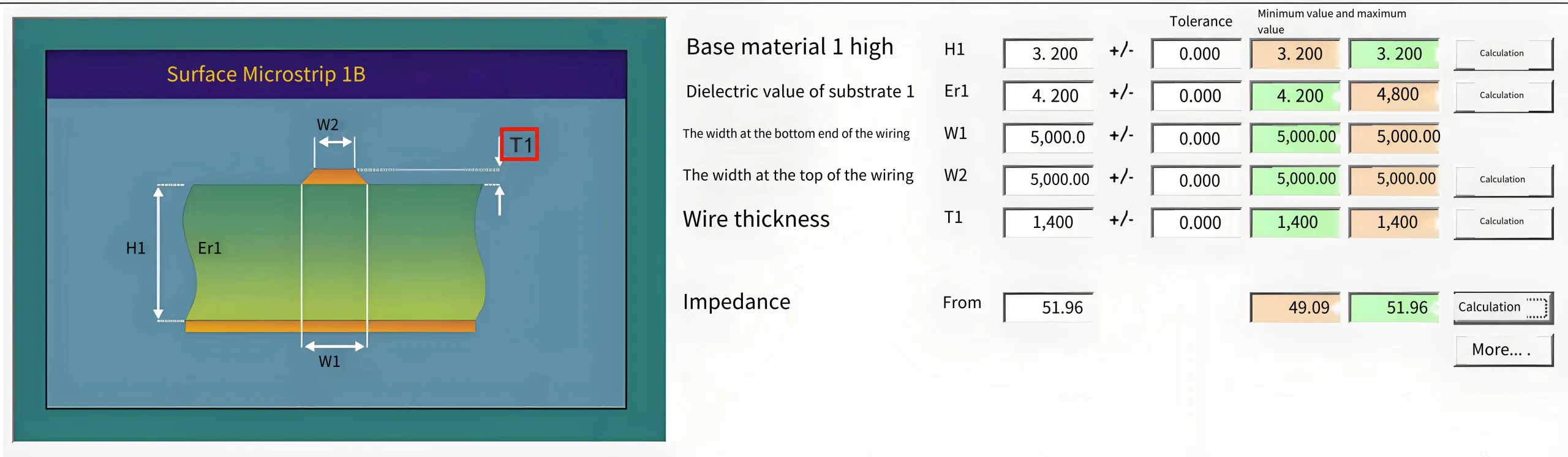
高速設計において, PCB トレースはもはや単純な電気接続ではなく、正確に制御された伝送ラインである必要があります. 特性インピーダンスの偏差 (例えば。, 50Ω シングルエンド, 90Ω/100Ω差動) 信号反射を直接引き起こす, オーバーシュート, データ・アイ・ダイアグラムのクロージャー. インピーダンスは主に配線幅に依存します (w), 誘電体の厚さ (H), 誘電率 (εr), および銅の厚さ. Polar Si9000 などの業界標準ツールは、簡略化された公式を使用してこれをモデル化します。 (マイクロストリップライン用):
Z0 ≈ (87 / √(εr + 1.41)) * ln(5.98 * H / (0.8 * W + T))
ここで、T はトレースの厚さです. 一般的なFR-4材の場合 (εr ≈ 4.2 @ 1GHz), 誘電体の厚さ H=5 ミルで 50Ω インピーダンスを達成するには, トレース幅 W は約 8.5 ミル. しかし, 高層番手基板の積層構造の不均一性, ガラス織り効果, および製造時のエッチング公差 (通常±10%) すべてがインピーダンスの変動を引き起こします. IPC-6012D 規格では、インピーダンス制御ボードの公称インピーダンスからの測定値の ±10% の偏差が許容されます。, しかし、ハイエンドアプリケーションでは±7%という厳しい公差が要求されるようになりました。.

パワーインテグリティとPCBの熱管理
レイヤー数が増えると, 配電ネットワークの複雑さ (PDN) デザインは飛躍的に成長する. コア電圧は0.8Vまで低くなり、過渡電流は数百アンペアに達します. このシナリオでは, 電源プレーンのターゲット インピーダンスは非常に低くなければなりません (例えば。, <1 mΩ) 電圧リップルを抑える. これには、デカップリング コンデンサの配置を慎重に計画する必要があります。, 電源プレーンとグランドプレーン間のプレーン間容量の最適化 (によって計算される C = ε0 * εr * A / d, ここで、A は重複領域、d は誘電体の厚さです。), 専用の電源層が必要になる場合があります. さらに, 高密度配線による電力密度の向上 (それを超える 100 一部の ASIC 領域の W/cm²) サーマルビアアレイによる冷却強化が必要, 埋め込まれた銅貨, または金属基板, スタックアップの設計と処理がさらに複雑になる.
PCB製造の錬金術: 多層基板向けの精密プロセスチェーン
設計を物理的な現実に変換することは、層数の多い PCB にとってもう 1 つの大きな課題になります. The core process can be summarized as a precise cycle of “lamination – alignment – drilling – plating.”
レイヤー間の位置合わせ: ミクロンレベルの登録技術
多層基板の全層 (内層コアとプリプレグ) 高温高圧下で単一ユニットに積層する必要がある. レイヤーの位置ずれにより、ドリルでトレースが切断される可能性があります, ショートパンツを作成する, またはインピーダンスの不連続を引き起こす. 16層基板の場合, 層ごとの平均アライメント誤差が 25 μm (IPC-A-600Gクラスで許容されるグラフィックレジストレーション許容値 3), 最悪の場合の累積誤差は次の値を超える可能性があります 100 μm - を損なうのに十分な量 0.2 mm BGA パッド.
UGPCB のような大手メーカーは、次の方法を使用してこの課題に取り組んでいます。 レーザー直接イメージング (LDI) そして 高精度光学アライメントシステム. 位置合わせピン そして グローバル基準スケール 各コア層にエッチング, CCDビジョンキャプチャとサーボ調整を組み合わせた, 内部のレイヤー間の登録を制御できます 15 μm (主要な業界ベンダーのプロセスに関するホワイトペーパーに基づくデータ). さらに, 材料レオロジー分析 積層中のプリプレグの樹脂の流れとガラス繊維の配向を予測することで、寸法変形を事前に補正できます。, プレス後の誘電体の厚さを均一にする.
https://example.com/pcb-lamination-alignment.png
画像の代替テキスト: 多層基板の積層・位置合わせ工程を詳しく解説, レーザーターゲットの表示, 光学的アライメント, そしてラミネートフロー, 高精度のレイヤー間の位置合わせを保証します.
相互接続経由: スルーホールから任意のレイヤーの HDI まで
従来のスルーホールは基板の厚さ全体を貫通します, 層数の多い PCB でかなりの配線スペースを占有し、長い信号リターンパスの問題を引き起こす. したがって, 高密度相互接続 (HDI) テクノロジー を使用して、より柔軟なレイヤー移行を可能にします。 ブラインドビア (表面から内層まで), 埋め込みビア (内層から内層へ), そして マイクロバイアス (直径 ≤ 0.15 mm).
例えば, a “1+N+1” HDI structure (表面層はマイクロビアを使用し、中央はN層の従来のコアです。) 配線密度を大幅に高めることができます 40% 総レイヤー数を増やすことなく (IPC-2226 HDI 設計標準を参照). しかし, これにより、次のようなプロセスの複雑さが生じます。 連続積層穴あけ加工, 充填とメッキを介して, そして 複数のラミネートサイクル. メーカーが装備しなければならない レーザーボール盤 (マイクロビア用), 縦型真空栓機 (空隙のない充填を保証するため), そして プラズマ洗浄装置 (ドリルの汚れを除去するには), そして厳格に実行する 飛行プローブ試験 そして 4線式ケルビン試験 すべての相互接続ポイントの信頼性を検証する.
将来の傾向: 材料イノベーションとシミュレーション主導の設計と製造の統合
高層数 PCB の進化は続く. PAM4 変調を使用して信号速度が 56Gbps 以上に進むにつれて, 低損失材料 (パナソニックのメグトロンのような 6, Rogers RO4000シリーズ) εr が次のように低い場合 3.2 および散逸係数 (Df) 下に 0.002 採用されています. 同時に, 埋め込みコンポーネント (埋め込み抵抗やコンデンサなど) そして 半導体パッケージの統合 (例えば。, インテルのEMIB, TSMCのSoIC) PCB と IC の間の境界線があいまいになりつつある.
設計者および調達スペシャリスト向け, 資格のある人を選ぶ 高い層数 PCBサプライヤー 最も重要です. 彼らに焦点を当てるだけでなく、 最大レイヤー能力 (例えば。, 安定した量産が可能 32 レイヤー), インピーダンス制御 能力 (インピーダンステストレポートを提供しているかどうか), そして HDIプロセスレベル (最小穴サイズ/トレース幅), 彼らを評価することが重要です 設計支援サービス (SI/PIシミュレーションやスタックアップ最適化アドバイスなど) そして 品質管理システム (IPCクラスへの準拠 3 AOI などの総合検査装置の規格と利用可能性, AVI, 3D X線).

高い信頼性を求めて, 高性能 多層PCB 解決? 設計シミュレーションから精密製造までのフルチェーン機能を備えた専門サプライヤーに連絡して、 カスタムスタックアップデザイン提案 そして 即時見積もり あなたのプロジェクトは成功への重要な第一歩です. Internet of Everything と計算爆発の時代に, 層数の多い PCB はもはや単なるキャリアではありません; それらは電子システムの性能限界を定義する基礎となるものです.