
BGAはんだパッドのわずか0.5mm²の亀裂は、プレミアムスマートフォンをにレンガすることができます “白い画面のペーパー級” - 従来のアンダーフィルカプセル化は、この重要なPCBの信頼性の脅威を偽装するだけです. スマートフォンが超薄いデザインと高性能の仕様に向けて急速に進化するにつれて, BGAパッドの割れ ダモクレスになりました’ 剣がぶら下がっています プリント基板 製造業. a $1,000+ 携帯電話 PCBアセンブリ マイクロクラックまたは市場のリターンレートの急増のためにスクラップになる 30% から タイプV骨折, 私たちは尋ねなければなりません: 本当に究極のソリューションです?
1. BGAパッドの割れ: エレクトロニクスの目に見えない殺人者
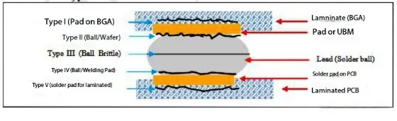
H3: 1.1 障害定義 & 5つの骨折タイプ
BGAパッドの割れ 間の分離を指します ICチップ 機械/熱応力下のPCBパッド. 5つの骨折タイプは、場所ごとに分類されます:
| タイプ | 失敗の場所 | 有病率 | プライマリトリガー |
|---|---|---|---|
| タイプI | チップ基板 層 | 12% | タンブリングテスト, 機械的ショック |
| タイプII | BGAパッドソルダーインターフェイス | 18% | サーマルサイクリング |
| タイプIII | リードフリーのはんだボール | 25% | ドロップインパクト, サーマルショック |
| タイプIV | はんだ-PCBパッドジョイント | 28% | リフロープロファイルの不一致 |
| タイプv | パッドサブストレート分離 | 17% | 構造変形, 物質的な劣化 |
1.2 ステルス性 & 破壊的な影響
従来のSMT検査検出 <5% に起因するパッド亀裂の:
-
マイクロクラックサイズ (5-50μm) 多層PCBで不明瞭
-
骨折にもかかわらず、電気の連続性はしばしば維持されます
-
アンダーフィルは、伝播を止めることなく亀裂を隠します, 再作業中に破壊的な除去が必要です

2. PCBAワークフロー全体の根本原因分析
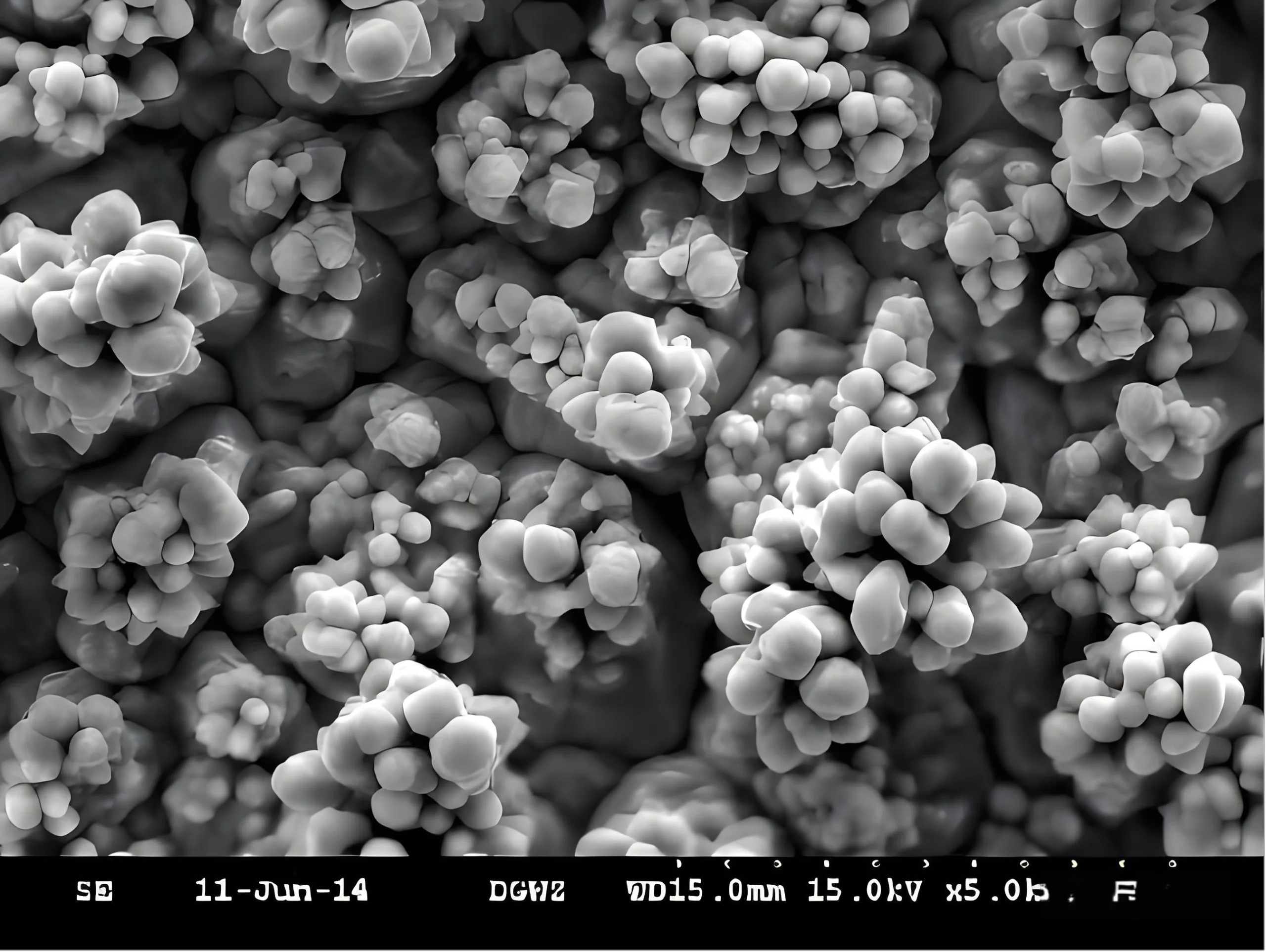
2.1 材料起源: 銅箔の結晶構造の発散
実験データが明らかになります: 特殊な銅箔 “ブドウのような” 結節構造が配信されます 18.5% 従来の結晶よりも高い接着.
2.2 PCB基板 制限: FR4の熱耐久危機
鉛フリーのはんだ付けは、248°Cのピーク温度です (+33°C対従来のプロセス). 標準FR4 130-140°CのTG 原因:
-
Z軸CTE >300 ppm/°C
-
T288デラミネーション時間 <3 分 (業界に必要です >5 分)
重要な式: 熱応力= e×α×Δt
どこ:
σ=熱応力 (MPa), E =弾性率 (GPA),
α= CTE (ppm/°C), ΔT=温度変化 (℃)
*ΔT= 100°Cで1.8×より多くの応力を生成する高いCTE基板*
2.3 プリント基板設計 落とし穴: 見落とされた機械的ストレス
の分析 7,000 ロシアの市場で失敗したユニットが示しています:
-
0.80MMボードは、3.2×1.00mmを超えるボードに障害を失いました
-
Tカードスロットにより、PCBAの亀裂リスクが増加しました 47%
-
BGAゾーンの下の大きな成分は、非対称の熱変形を引き起こしました
3. 重要なPCBプロセス制御のブレークスルー
3.1 PCB製造最適化マトリックス
| プロセス | 従来の | 最適化 | 改善 |
|---|---|---|---|
| 銅箔 | 標準的な結節 | ブドウのような結晶 | 接着↑18.5% |
| メッキの厚さ | 18-23μm | ≥30μm | 引張↑32% |
| 表面準備 | ベルトサンディング | マイクロエッチ + スプレー | 銅損失↓60% |
| はんだマスクの開口部 | 円形 | 六角 | 貼り付けフロー↑40% |
3.2 リフロープロファイル革命
故障ルート: 標準リフローは、190°C→130°Cからの12秒の冷却のみを費やします, 急速な収縮を引き起こします.
解決: TGより上に滞留時間を延長します 150%, により熱応力を減らす 35%.
4. 包括的なPCBAソリューションデータベース
4.1 デザインの革新
-
パッドジオメトリ: 周辺パッドを楕円形に変換します (長軸 +0.1mm)
-
スタックアップデザイン: BGAの下に局所的な銅バランス層を追加します
-
クリアランスルール: 大規模な禁止 コンポーネント BGAゾーンから3mm以内
4.2 マテリアルアップグレードパス
-
Tg≥170°CでFR4を指定します
-
銅箔RZを制御します (粗さ) 3.5〜5.0μm
-
低文字を採用します (<2.5%) 高タフネス樹脂システム
4.3 プロセス制御レッドライン
-
30μm以上の銅メッキ (検証)
-
OSPパネル間隔 >5mm (酸トラップ予防)
-
テストフィクスチャー圧力≤7kg/cm², ピンライフ <500Kサイクル
-
150-180°Cリフローゾーンは90秒以上住んでいます
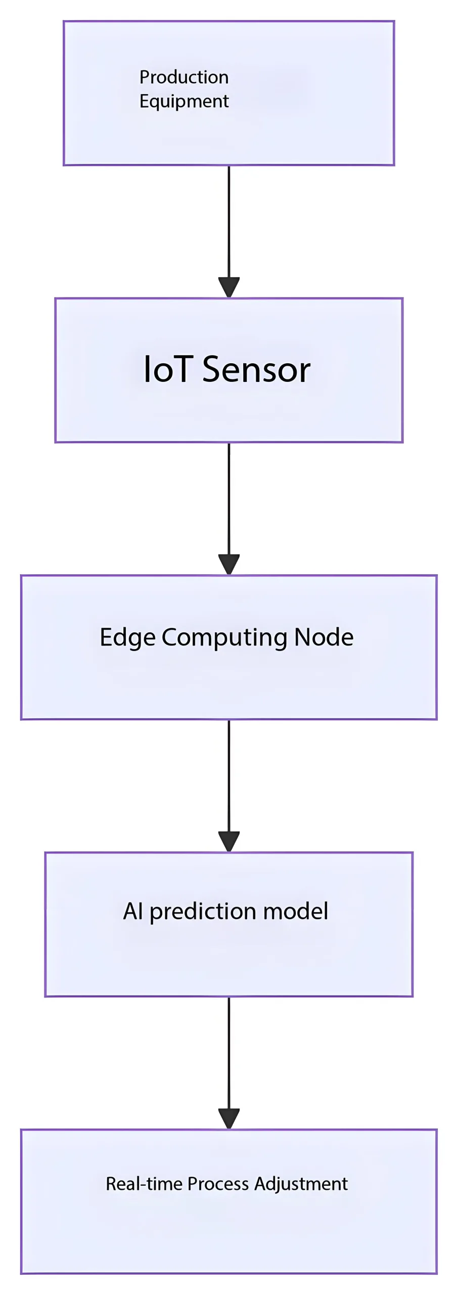
5. 将来のテクノロジーロードマップ
として HDI PCB 0.4mmの厚さに向かって前進し、BGAパッドは0.2mm未満を縮小します, ブレークスルーが必要です:
-
ナノスケールの銅治療: マグネトロンスタード接着層
-
CTE適応基質: 温度応答性ポリマー複合材料
-
AIプロセス監視: リアルタイムはんだジョイントヘルス予測
結論: 信頼性はで設計されています
BGAパッドクラッキングが構成されます システムレベルの信頼性の障害. 実装後の結果:
-
タンブリングテスト合格率: 82% → 99.6%
-
市場のリターン率: ↓70%
-
コスト削減: $1.20/アンダーフィルエリミネーションによるボード
*覚えて: パッドあたりの接着が0.1kgf増加すると、指数関数的な信頼性が向上します. これはプロセスの改良を超越します - それはゼロ欠陥のある製造の究極の追求を具体化します。*
はんだパッドの顕微鏡領域で, ブドウのような銅結晶は、ナノスケールの保護ネットワークを織ります, リードフリーの球体が六角形のマスクの開口部内で精密なダンスを実行する一方. エレクトロニクスの信頼性革命は、0.01mmごとに揺るぎないコミットメントから始まります.
