
導入: 嵐の目の財団
半導体産業に注目が集まる, の プリント基板 (プリント基板) 長い間沈黙の役割を果たしてきた, 基礎の柱. しかし, で 2025, 原材料価格の嵐, 金および銅張りのラミネートを中心とする (CCL), PCBをサプライチェーンのコスト圧力の最前線に押し上げてきた. この嵐は偶然ではありません; これは、AI インフラストラクチャの拡大による急激な需要の増加と、限られた供給能力との間の激しい衝突です。. この記事では、PCB 業界のコスト課題とその根底にある要因について専門的な分析を提供します。, 危機の中でいかに深刻な技術変革が価値の飛躍を可能にしているかを明らかにする. 信頼性の高い情報を求める企業に重要な洞察を提供します。 PCBサプライヤー および高品質 プリント基板 サービス.
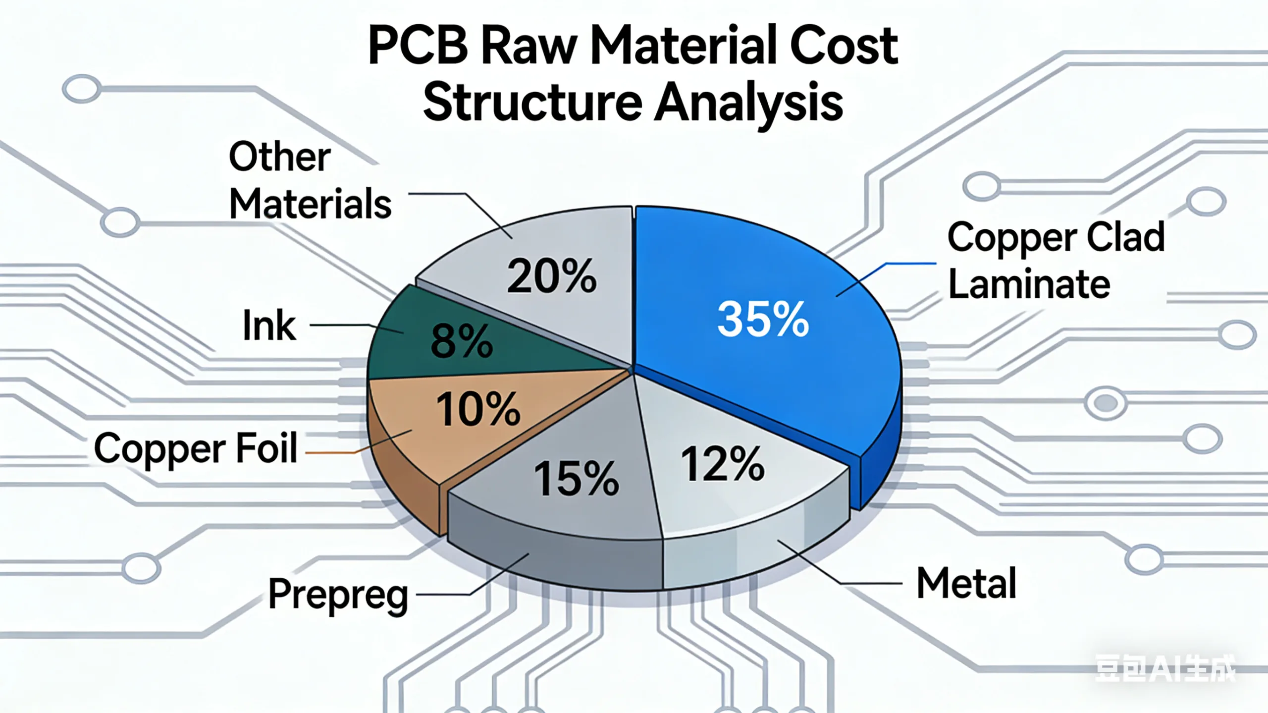
私. コストの分解: The “Gold and Silver” Straws Breaking the Camel’s Back
原材料のコスト構造 プリント基板 複雑です, but gold and copper-clad laminates are undoubtedly the two heaviest “weighted stocks.” According to analysis from the authoritative industry firm Prismark, 典型的な多層では サーバー用基板, CCL は次のことを説明できます。 30%-40% 費用の, 一方、金などの貴金属はメッキや表面仕上げに使用されます。 (例えば。, 同意する) 説明できる 8%-15%. 一緒に, 総材料費の半分に近づきます. これは次のように単純化できます:
PCB原材料費 ≈ (CCLコスト×シェア) + (貴金属原価×シェア) + (その他の材料費)
(ソース: プリズムマーク Q3 2025 PCB材料コスト分析レポート)
1. 金: 光沢のある仕上がり以上のもの
ハイエンドのゴールド プリント基板 優れた導電性を確保するために、主に重要な接続部の表面仕上げに使用されます。, 耐酸化性, およびはんだし. シアン化金カリウムの価格 (金の塩), 例えば, 業界のバロメーターとなっている. 韓国の大手企業のデータ PCBメーカー 驚異的な軌道を描く: およそから 50,000 KRW/グラムインチ 2023 に 99,000 2025 年第 3 四半期の KRW/グラム — ほぼ 100% 増加. これは製造コストの上昇に直結します。 HDI PCB ENIG などのプロセスを使用した IC 基板 (エレクトロレスニッケルイマージョンゴールド). 大量の取引を必要とするクライアント向け PCBAアセンブリ, このコスト移転は重要です.
2. 銅張積層板: AI 需要の直接的なパイプライン
回路パターンを運ぶコア誘電体として, CCLのパフォーマンスが最終的な勝敗を直接左右します。 PCB 信号の完全性, 熱管理, と信頼性. AIサーバー, 高速スイッチ, そして AI アクセラレータ カード データスループットと信号損失に関してほぼ厳しい要件を課す, 爆発的な高速・高周波需要を促進, 超低損失 (例えば。, 超低損失, 非常に低損失グレード) ラミネート.
Samsung Electro-Mechanics などの一流メーカーからのフィードバック - 10%-15% 第 3 四半期の調達コストの前年比上昇 - この構造的な供給緊張を象徴する. これは、以下の分野で使用される高性能ラミネートに特に当てはまります。 AIサーバーのマザーボード そして GPU アクセラレータ カード PCB.

Ⅱ. 根深いドライバー: PCB の需要マップを再構築する AI の熱狂
原材料費の高騰が表面症状; コアエンジンはグローバルなデジタルとインテリジェントな変革です, 特にAIコンピューティングインフラストラクチャにおける軍拡競争.
1. 役割の進化: From “Connector” to “System-Critical Component”
伝統的に, プリント基板 コンポーネントの機械的サポートおよび電気接続プラットフォームと見なされていました. AI時代に, この役割は根本的に変わりました. 次世代アーキテクチャ, NVIDIA の Rubin などのプラットフォームが代表例, 極めて高い内部相互接続帯域幅と密度を追求する, レイヤー数を増やす プリント基板 (通常 22+ レイヤー) そして 任意の層HDI 技術標準. 上のすべての痕跡 プリント基板 データ遅延と消費電力に影響を与える; その設計と製造の精度は、CPU/GPU 間の相乗効率に直接影響します。, メモリ, そして加速器. 業界分析によると、 AIサーバーのマザーボード 値は標準サーバーの倍数です, そので プリント基板部 それに応じて技術内容と価格も上昇するとみられる.
2. 需要の急激な増加仕様
AI のトレーニングと推論により、具体的かつ厳格なデータが生成されます PCB 要件:
-
レイヤー数の増加: より複雑な電力供給ネットワークとより多くの信号層に対応するため, AIサーバーマザーボード レイヤー数は増加傾向にあります 30 レイヤーとその先へ.
-
マテリアルのアップグレード: データレートが 224Gbps 以降に移行し、M6 の需要が高まっています, M7 グレードの超低損失ラミネート (Df は次のように低い 0.0015).
-
サイズ & 統合: より多くのコンピューティングユニットを統合するためのより大きなボードサイズ, 組み込みコンポーネントなどの高度なプロセス プリント基板 統合とパフォーマンスを強化するため.
によると、 IPC (エレクトロニクス産業をつなぐ協会) 2025 展望レポート, 世界的なハイエンド プリント基板市場 データセンターと AI インフラストラクチャ向けの CAGR は 100% 以上になると予測されています 14% から 2024 に 2028, 業界平均をはるかに上回っている.
Ⅲ. バリューリープ: 技術変革を通じて前進する道
Facing “crushing costs,” leading PCBメーカー 受け身で我慢するのではなく、技術の高みに向かって積極的に前進する, 製品価値の変革を通じてプレッシャーを解決し、新たな市場を開拓する.
1. ハイエンド製品ポートフォリオへの戦略的転換
“Pursuing profitability through high value-added products” is the industry consensus. 主要な経路には以下が含まれます:
-
先進的なパッケージング基板に注力: チップレットとヘテロジニアス統合がトレンドになる中, FC-BGA用基板の需要 (フリップチップボールグリッドアレイ) 梱包材が急増中. これらの基板は、非常に細い線幅/間隔を特徴としています。 (10μmまで/10μm以下), 高い技術的障壁が存在する, より大きな利益率を提供します.
-
次世代メモリ インターフェイスに賭ける: 1cナノメートルプロセスに基づくDRAM, を中心に商品化を目指す 2026, ~の需要を促進するだろう プリント基板 8Gbps+のDDR5メモリインターフェイスをサポート. さらに, SoCAMM PCB (圧縮接続メモリモジュール), AIサーバー向けに調整された将来のメモリソリューション, ~の新たな成長点を表す プリント基板設計 と製造.
-
ASIC の波を受け入れる: 自社製AIチップ (ASIC) Googleのようなクラウド大手から, アマゾン, と Microsoft はカスタマイズされた高密度相互接続の需要を促進しています (HDI) ASIC基板. 高速性を重視した製品です, 密度, と信頼性, のフロントエンドにおける典型的な高価値通信事業者を表します。 プリント基板 プロセス.
2. イノベーションによる費用対効果の最適化
単にコストを転嫁するだけでは持続可能ではない. 技術革新によるコスト効率の向上が主要な差別化要因です.
-
設計最適化: 高度なシミュレーション ツールを使用してレイアウト設計を最適化する, パフォーマンスを保証しながら、層数を減らすか、よりコスト効率の高い代替材料を採用する可能性があります。.
-
プロセスイノベーション: 製造プロセスを改善して材料利用率を高める (例えば。, CCLパネルの最適化) 金の厚さを信頼できる最小限の基準まで減らす (従う IPC-4552/4556 仕様).
-
サプライチェーンのコラボレーション: ラミネートおよび化学品のサプライヤーと戦略的パートナーシップを確立し、パフォーマンスとコストのバランスをとったカスタマイズされた材料ソリューションを共同開発します。.
Rの場合&D 企業が要求する PCBプロトタイピング そして少量 PCBAの生産, これらのハイエンド経路における統合された設計、製造、組立サービスと専門知識を提供するパートナーを選択することが重要です.

Ⅳ. 今後の展望: 2026, PCB 値リモデリングの変曲点
2026 今年は世界における価値観の刷新にとって極めて重要な年であると広く考えられています。 プリント基板産業. 一方で, 新しい生産能力の稼働により、原材料コストの圧力が部分的に緩和される可能性がある. さらに重要なことは, AIによるテクノロジーのアップグレードから得られる利益, HPC (高性能コンピューティング), そして高速通信 (例えば。, 5.51G/6G) 完全に明らかになるだろう.
のメトリクス PCB値 will evolve from “price per square meter” more toward “cost per unit of bandwidth” or “cost per watt of efficiency.” PCBメーカー シグナルインテグリティに関する深い専門知識を備えたシステムレベルのソリューションを提供できる, パワーの完全性, そして熱管理は決定的な競争上の優位性を保持します.
結論: 嵐の目に堀を築く
なんと プリント基板産業 is experiencing is “growing pains” fueled by strong demand and accompanied by profound technological change. 金とラミネートの価格変動は、この壮大な物語の中で最も顕著な章にすぎません. 核心的な話は、 プリント基板 エレクトロニクス分野の舞台裏から表舞台に移りつつある, そのパフォーマンスはハイエンド コンピューティング システムの上限を直接決定します。.
家電ブランドやR向け&D社, 今こそ再評価する時だ PCB調達戦略 そして PCBA パートナー. 単なる単価を超えて, サプライヤーの技術力と多層基板の量産経験をより深く評価する, 高速材料塗布, 高度なパッケージング相互接続が不可欠です. 先進的なテクノロジーリーダーと提携して、コストの課題に対して設計を共同最適化することが、将来の市場で勝つための鍵となる.
今すぐ専門の PCB/PCBA サプライヤーに問い合わせて、次世代 AI のカスタマイズされた回路ソリューションと正確な見積もりを入手してください。, データセンター, またはハイエンド通信製品, このテクノロジーの急増で主導権を握ります.