
1. PCBテクノロジーの進化とイノベーションドライバー
The プリント基板 (プリント基板) として機能します “電子製品の母,” 銅の痕跡とパッドを介したコンポーネントの機械的固定と電気接続を有効にする. 最新のPCBは、単一層ボードから高密度の相互接続に進化しました (HDI) およびマルチレイヤーボード, 高性能の要求に駆られます, 小型化, と信頼性.
主要な市場ドライバー:
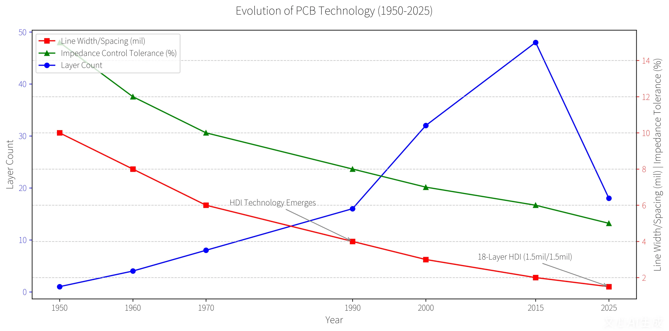
- AIサーバーの需要が急増しました 60% ヨイイン 2025, HDIをブーストします 多層PCB 採択.
- 自動車電子浸透, 特にEVで, 燃料補給高度の信頼性PCB成長.
- UGPCBの10層の1次PCBは、信号損失を減らします 42% 2milトレースとレーザーマイクロビアテクノロジーを使用します.
技術的なブレークスルー:
- トレース幅/1.5mil/1.5milという低い間隔 (業界平均: 3ミル).
- ±5%のインピーダンス制御耐性 (業界標準を超えています 10%).
2. PCB分類とアプリケーション
2.1 レイヤーベースの分類
単層PCB: シンプルなデザイン (例えば。, おもちゃ, パワーアダプター).
二重層のPCB: 相互接続にVIASを使用します; ルーターや家電製品に最適です.
多層PCB (3+ レイヤー): スマートフォンの高密度設計, 自動車システム, および産業コントローラー.
2.2 材料 & プロセスベースの分類
リジッドPCB: 固定型デバイス用のFR-4基板 (電話, テレビ).
柔軟なPCB (FPC): 曲げ可能な用途向けのポリイミドベース (画面ケーブル, ウェアラブル).
剛体PCB: 複雑なアセンブリ用の剛性と柔軟なセクションを組み合わせます (ドローン, 医療機器).
3. アプリケーション固有の要件
3.1 家電
- スマートフォン: 12-CPUの剛性PCBを層化します, カメラ, およびRFモジュール.
- ラップトップ: 6-10 CPUのレイヤーボード; バッテリー接続用のFPC.
3.2 産業用電子機器
- PLCコントローラー: 4-6 モーター制御のためのEMC抵抗を備えたPCBを層にします.
- センサー: 過酷な環境での安定した信号伝達を備えた二重層ボード.
3.3 カーエレクトロニクス
- EVバッテリー管理: 電圧/温度監視用の多層PCB.
- ADASシステム: ミリ秒レベルの応答を備えた高解放性ボード.
3.4 ハイエンドアプリケーション
- 5Gベースステーション: 8-12 高周波信号の整合性のためのRFボードをレイヤーします.
- 医療機器: ECGマシン用の生体適合性材料を備えた多層PCB.
4. 市場データと成長予測
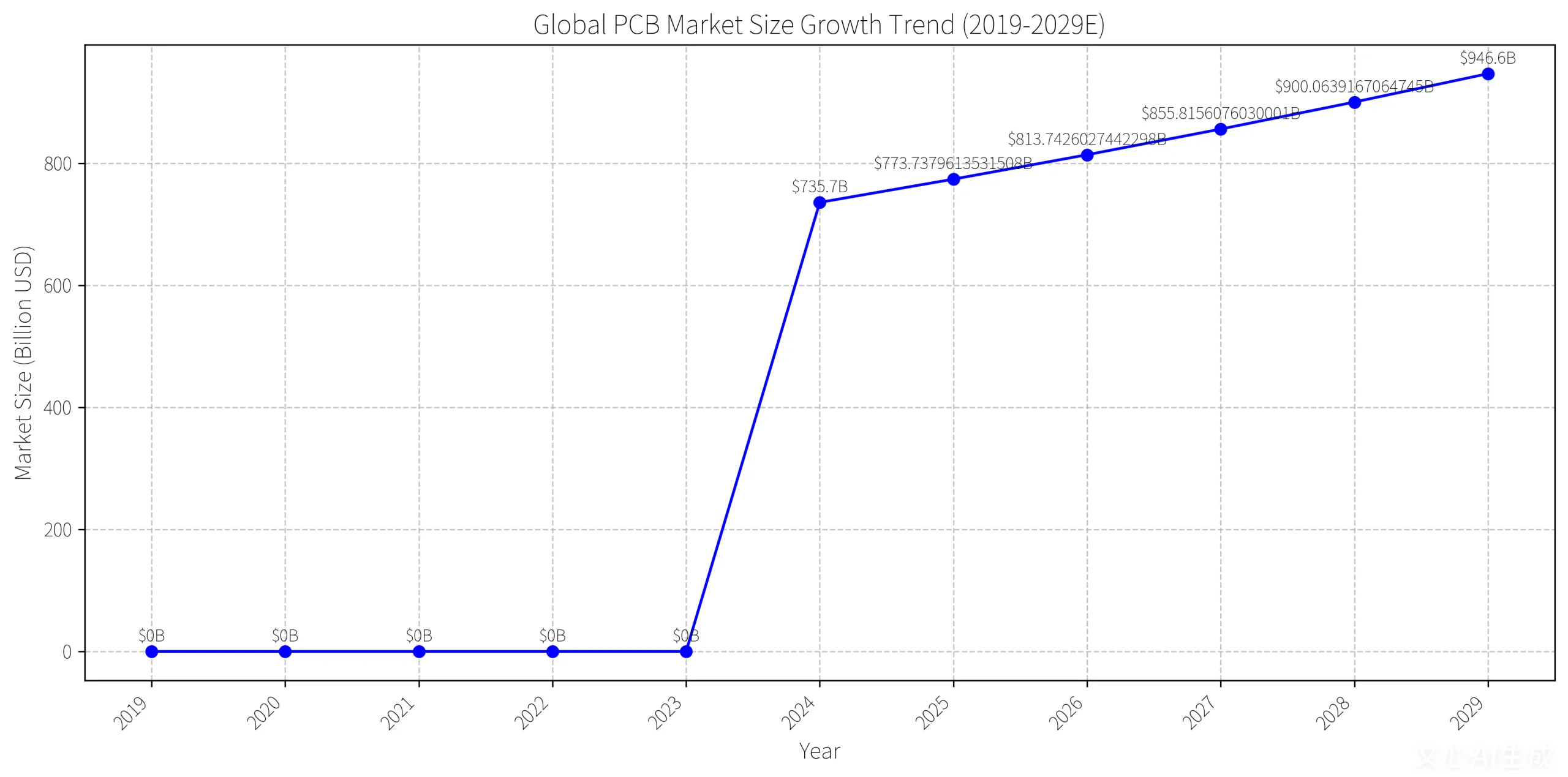
- グローバルPCB市場: 155.38b by 2037.
- HDIボード: 33.4% 市場シェア 2037, スマートフォンとAIサーバーによって駆動されます.
- 自動車PCB: 18.79b by 2035 (CAGR 5.5%).
中国の支配: のアカウント 50% グローバル生産の; 到達するハイエンドPCB 40% 共有 2025.
5. PCBおよびSMT Synergy
PCB設計と SMT (表面実装技術) 相互依存しています:
- PCBは、SMTコンポーネントに正確なはんだパッドレイアウトを提供します (例えば。, 0402 抵抗器: 0.4mm×0.2mm).
- SMTは高密度アセンブリを有効にします, スマートフォンPCBのBGAチップなど.
UGPCBの利点: LPKFレーザーイメージングシステムは、±25μmのアライメント精度を実現します, HDI生産にとって重要です.
6. 将来の課題と傾向
コスト圧力:
- 銅価格 15% で 2025;銅製のラミネート (CCL) コストは上昇しました 8-12%.
- 中小企業はマージン圧縮に直面しています, 業界の統合を加速します.
技術的変化:
- の需要の増加 8-16 PCBとIC基板を層化します (市場規模: $45b by 2025).
- 低電力, 環境に優しいデザインのための高温伝導材料.
グローバル拡張:
- 東南アジアに投資するPCBメーカー (ベトナム, タイ) コスト効率と関税回避のため.
結論
PCB業界は、グローバルエレクトロニクスにとって極めて重要です, AIによって駆動されます, 自動車, および5Gイノベーション. 企業は技術的なアップグレードを優先する必要があります, サプライチェーンの多様化, コストのボラティリティと地域競争の中で繁栄するためのグリーン製造.
