

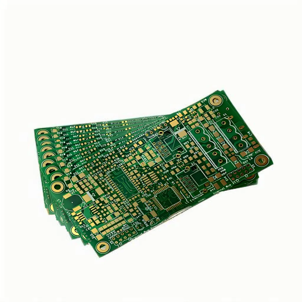
What is a 10Layers ENIG Board?
A 10-layer ENIG (エレクトロレスニッケルイマージョンゴールド) board is an advanced 多層プリント回路基板 (プリント基板) with ten layers of conductive material, typically copper, 絶縁層によって分離されています. The “ENIG” refers to the surface treatment applied to the copper traces, which involves electroless nickel and immersion gold plating. このタイプの プリント基板 is designed for high-density and complex electronic applications.


設計要件
Designing a 10-layer ENIG board involves several key considerations:
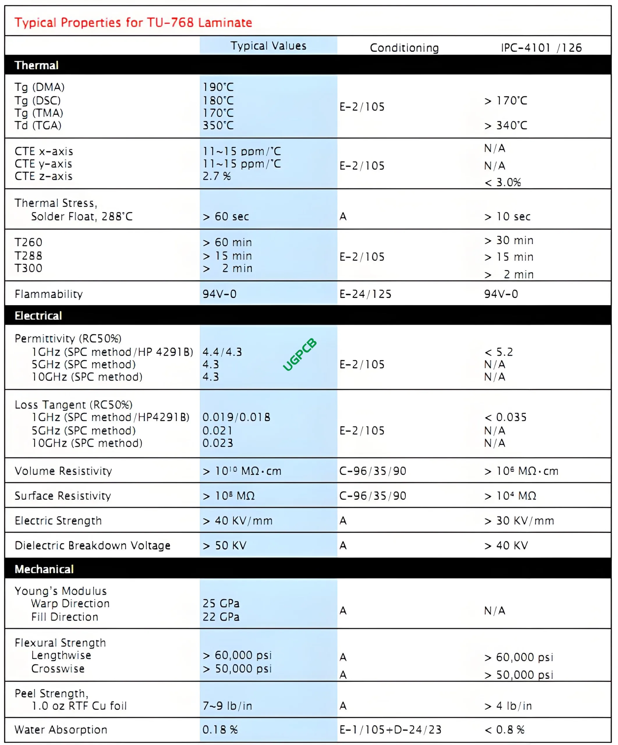
- 材料: Made from TU-768, a high-performance composite material known for its excellent electrical properties and durability.
- レイヤー数: Consists of ten layers, allowing for intricate and dense circuit designs.
- 銅の厚さ: Ranges from 2OZ to 3OZ, providing robust conductivity for high-power applications.
- 表面処理: Features immersion gold plating, which offers excellent solderability and corrosion resistance.
- トレースとスペース: Minimum trace and space are set at 3mil (0.075mm), enabling fine details in the circuit design.
How Does it Work?
The 10-layer ENIG board functions by providing multiple layers of conductive pathways, 絶縁層によって分離されています, to interconnect electronic components. The immersion gold surface treatment ensures reliable soldering and long-term protection against oxidation and wear.
アプリケーション


Due to their complexity and reliability, 10-layer ENIG boards are widely used in various high-end electronic applications including:
- 航空宇宙および防衛システム
- 高速ネットワーキング機器
- Advanced telecommunication devices
- 医用画像機器
分類
10-layer ENIG boards can be classified based on several factors:
- 素材によって: Most commonly made from TU-768 due to its balance of cost, 強さ, および電気的特性.
- By Copper Thickness: Varies from lightweight (2オズ) to heavyweight (3オズ) depending on the application’s needs.
- 表面処理による: Features immersion gold plating, which provides excellent solderability and corrosion resistance.

使用材料
The primary materials used in manufacturing 10-layer ENIG boards include:
- TU-768: A glass-reinforced epoxy laminate that provides excellent mechanical strength and thermal stability.
- 銅: Used for the conductive layers, with thickness varying based on design requirements.
- はんだマスク: Typically green or white, it protects the copper traces from oxidation and accidental short circuits.
- イマージョンゴールド: Applied as a surface treatment to improve solderability and protect against corrosion.
性能特性
Key performance attributes of a 10-layer ENIG board include:
- 高密度: Allows for more コンポーネント to be packed into a smaller area.
- 信頼性: The use of multiple layers reduces the risk of electrical shorts and improves signal integrity.
- 信号の完全性: Improved due to shorter signal paths and reduced crosstalk.
Structural Composition
構造的に, a 10-layer ENIG board comprises:
- Conductive Layers: Made of copper, etched into the desired circuit patterns.
- Insulating Layers: Prevent electrical shorts between conductive layers.
- Plated Through-Hole Vias: Facilitate connections between different layers.
特徴的な機能
Some notable features of a 10-layer ENIG board are:
- Fine Pitch: Allows for high-density interconnects making it ideal for compact devices.
- Robustness: The use of multiple layers provides a strong mechanical bond between the board and components.
- 多用途性: Suitable for a wide range of applications due to customizable layer counts and material choices.
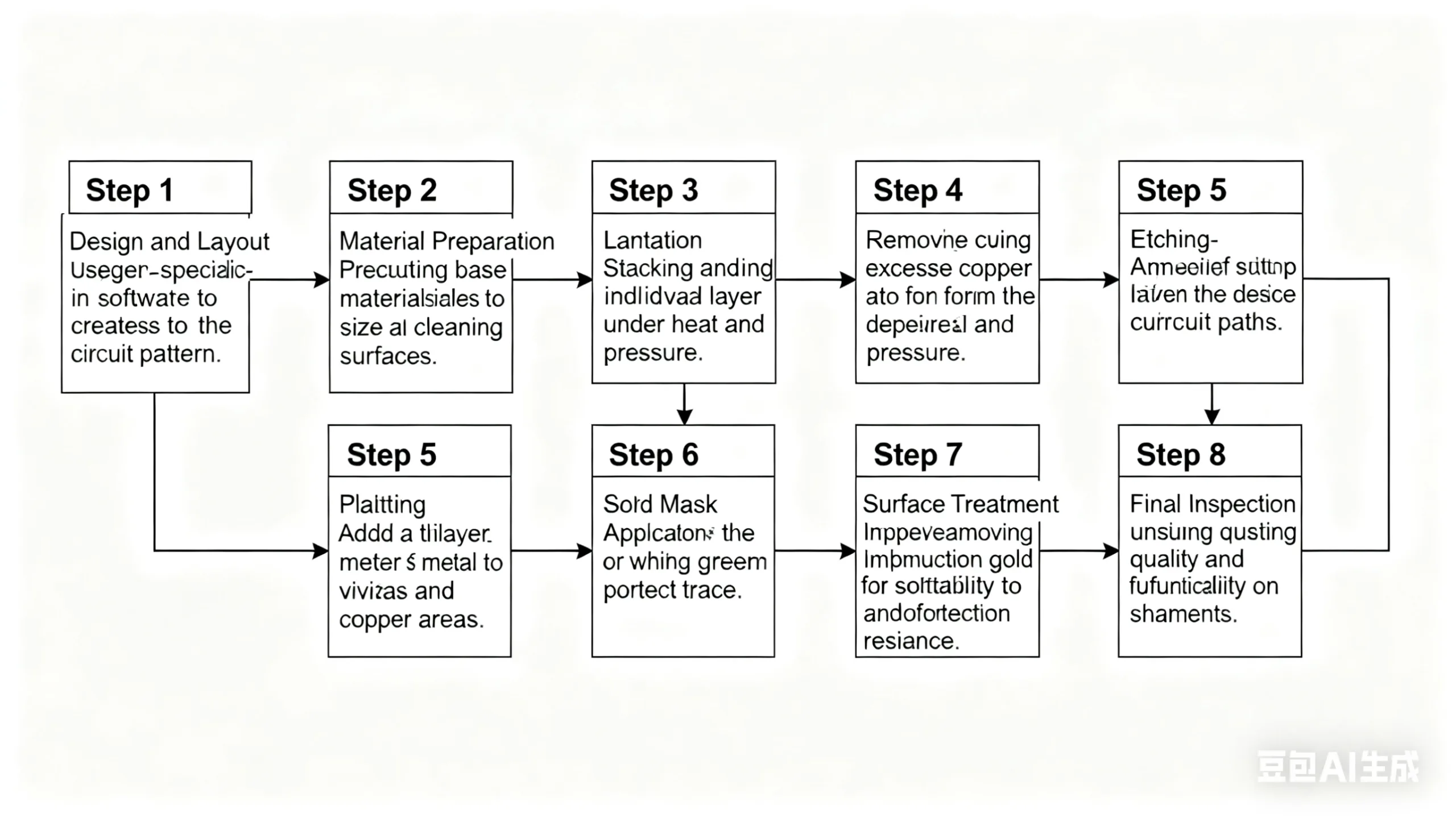
製造工程
The manufacturing process of a 10-layer ENIG board involves several steps:
- デザインとレイアウト: Using specialized software to create the circuit pattern.
- 材料の準備: Cutting base materials to size and cleaning surfaces.
- ラミネート加工: Stacking and bonding individual layers under heat and pressure.
- エッチング: Removing excess copper to form the desired circuit paths.
- メッキ: Adding a thin layer of metal to vias and exposed copper areas.
- ソルダーマスクの塗布: Applying the green or white coating to protect traces.
- 表面処理: Applying immersion gold for solderability and corrosion resistance.
- 最終検査: Ensuring quality and functionality before shipment.

ユースケース
Common scenarios where a 10-layer ENIG board might be employed include:
- High-density interconnect applications in aerospace and defense systems.
- Advanced communication systems requiring low signal loss.
- Portable medical instruments needing reliable performance in harsh environments.
- Automotive electronics demanding robustness and longevity.
要約すれば, the 10-layer ENIG board represents a significant advancement in printed circuit board technology offering unparalleled complexity and performance for modern electronic applications Its design flexibility combined with superior signal integrity and durability makes it an essential component in the development of next-generation high-end electronics and beyond