

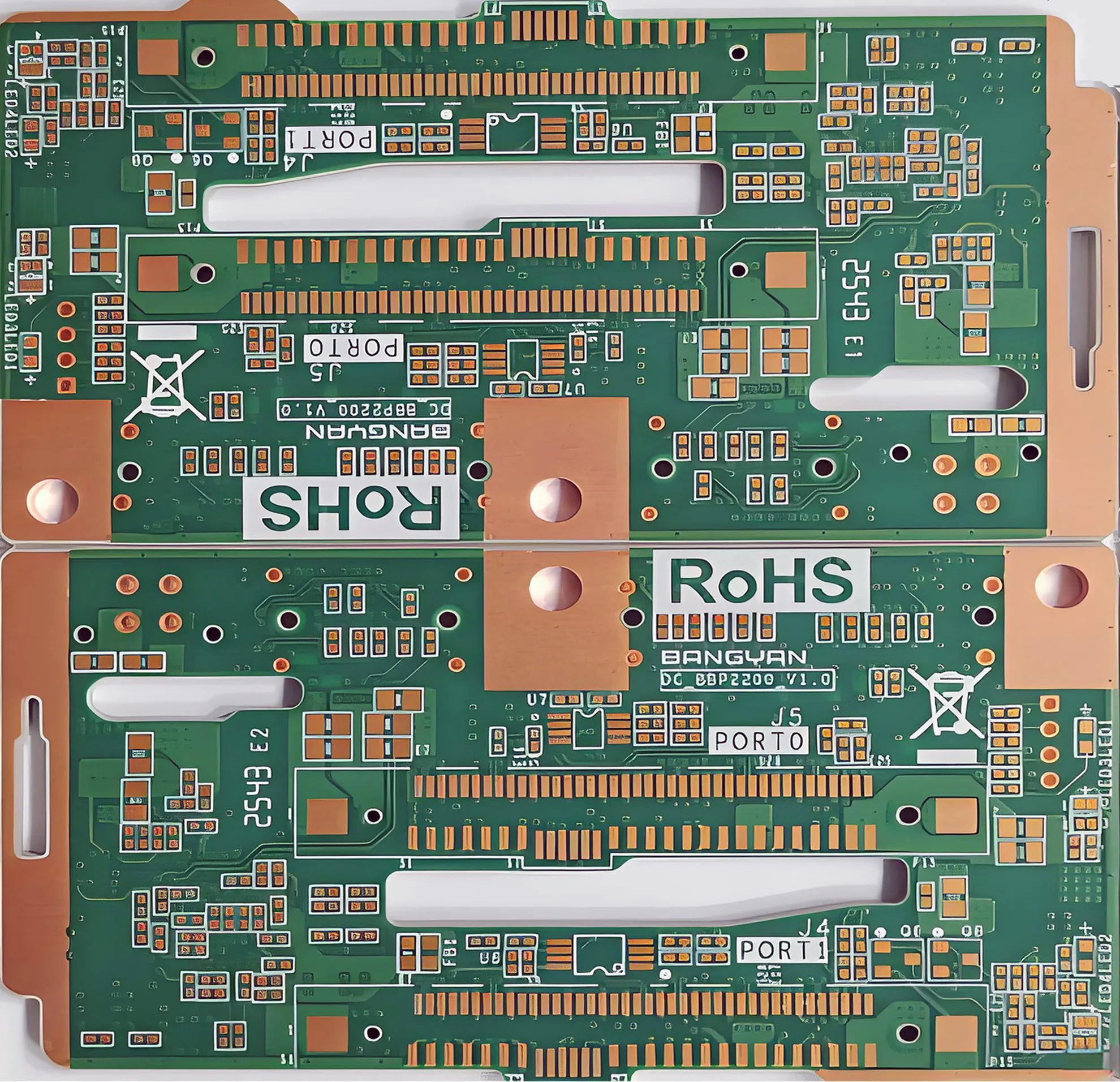
プロフェッショナル製品の概要: 12層の高速, 高密度PCB
高速データ伝送と複雑なシステム統合の時代へ, 従来のプリント基板 (プリント基板) 高度なエレクトロニクスの性能要求を満たすには至っていません. The 12-レイヤー高速, 高密度PCB 設計されたソリューションです. までの機能 12 正確に位置合わせされた導電層, コンパクトな設置面積内で複雑な相互接続と効率的な信号伝送が可能になります。, としての役割を果たす “中枢神経系” ハイエンドネットワーク機器向け, データセンターサーバー, ハイパフォーマンスコンピューティング (HPC), AIハードウェアと.
専門家として PCBメーカー そして PCBサプライヤー, UGPCB は高度なプロセスを活用して信頼性の高い製品を提供します 12-層 PCBボード 生産, 製品が競争力のあるパフォーマンスを維持できるようにする.
綿密なパラメータ分析: パフォーマンスの基礎
高品質の能力 多層プリント回路基板 仕様によって定義されます. 以下はこの製品のコアパラメータの分析です:
-
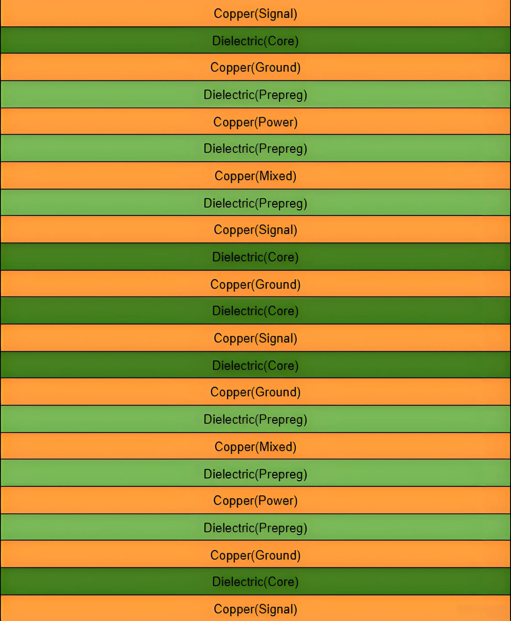
レイヤー数 & 積み重ね: 12 レイヤー. これ 多層PCB設計 優れたシグナルインテグリティを提供します (そして), パワーの完全性 (PI), 層数の少ないボードと比較した場合の EMC パフォーマンス. 専用の電源プレーンとグランドプレーンが可能になります, 高速信号にクリアなリターンパスを提供.
-
板厚 & 許容範囲: 2.4mm±10%. この堅牢な厚さにより、バックプレーンや大フォームファクターのアプリケーションに優れた機械的強度が提供されます。, 嵌合および取り付け時の信頼性を確保. 厳しい公差により組み立ての一貫性が保証されます.
-
完成銅重量: ユニークな分布:
1/1/1/1/1/2/2/1/1/1/1/1 oz. これは、内層が (L6 & L7) 2オンスの重銅を使用, 大電流電力供給用に特別に設計. 外側とその他の信号層には 1 オンスの銅を使用, ファインラインエッチング用に最適化. このハイブリッド構造が特徴です。 高信頼性 PCB製造. -
重要なプロセス能力:
-
最小ドリル穴サイズ: 0.2mm. 高密度 BGA ファンアウトをサポート, ルーティングの柔軟性の向上.
-
最小線幅/スペース: 0.076mm / 0.09mm (3ミル / 3.5ミル). 達成 高密度相互接続 (HDI)-レベルルーティング, 高速信号伝播に不可欠.
-
-
表面仕上げ: OSP (有機はんだ付け性防腐剤). 有鉛はんだ、鉛フリーはんだの両方に対応, 銅パッドを酸化から保護します, 優れた表面平坦性を実現, コスト効率が高く、高密度 SMT を備えたボードに最適です コンポーネント.
コア材料 & キーテクノロジー: 優れたシグナルインテグリティを実現
-
高性能ラミネート: 活用する ナンヤ NY6300S 高速ラミネート. 高いガラス転移温度 (TG >150℃) 高温リフローはんだ付け時の寸法安定性と信頼性を確保. 最適化された誘電率 (DK) および散逸率 (Df) 高周波での信号損失を大幅に低減, ~の物質的基盤を形成する 高周波プリント基板.
-
アドバンスト銅箔: 雇用する RTF (裏面処理箔) 銅. 標準電着塗装との比較 (編) ホイル, RTF フォイルの特徴はより滑らかです, 処理面の薄型表面. これにより、次のような信号損失が軽減されます。 “表皮効果” 高周波で, 差動信号のパフォーマンスを大幅に向上させます。 10 Gbps.
-
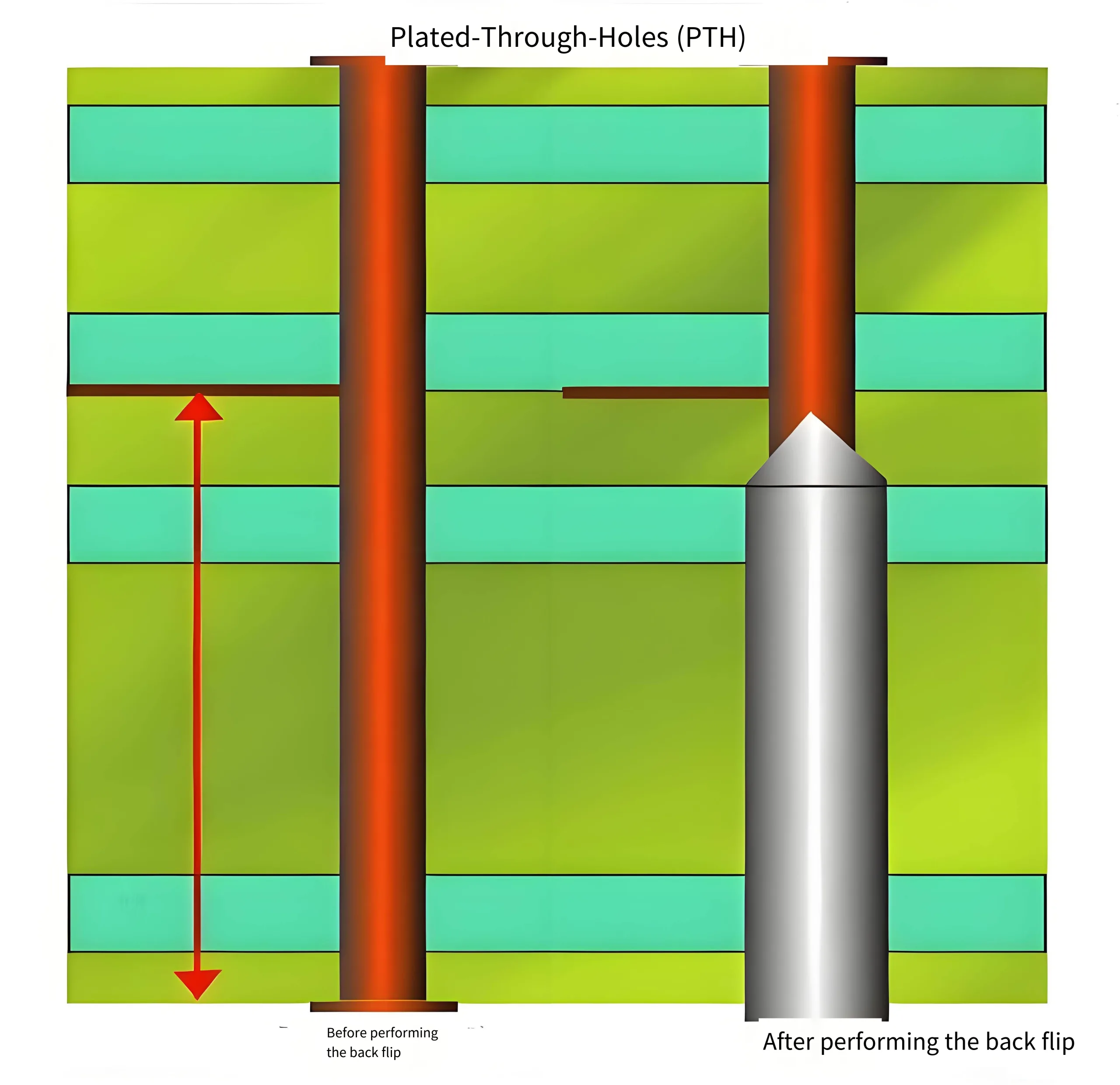
重要なプロセス: 制御された深さの穴あけ (バックドリリング): 12層以上の場合 多層PCB, 未使用部分 (スタブ) スルーホールビアは重大な信号反射を引き起こす可能性があります, 誠実さを損なう. The バックドリル加工 この機能しないスタブ経由を正確に削除します, 悪影響を排除するための重要なテクノロジー 高速多層PCB パフォーマンス.
生産フロー & 品質保証
UGPCB 12-層PCBの製造プロセス を厳守します IPC標準 そして含まれます 製造可能性のための設計 (DFM) レビュー, 内層イメージング, ラミネーション, 掘削 (バックドリルも含めて), メッキ, 外層イメージング, はんだマスクの塗布, 表面仕上げ (OSP), ルーティング, 電気試験, そして最終検査. 各ステージは精密測定装置によってサポートされています (あおい, インピーダンス試験, フライングプローブテスト), すべてを保証する 回路基板 納入された製品は設計仕様と当社の高品質基準を満たしています.
典型的なアプリケーション & 製品分類
この高性能な PCBボード 要求の厳しい電気環境や複雑なシステム向けに設計されています, 主にで使用される:
-
ハイエンドネットワーク & 通信機器: 400G/800G光モジュール用コアマザーボード, ハイエンドルーター, とスイッチ.
-
データセンター & クラウドコンピューティング: サーバーのマザーボード, アクセラレータカード, ストレージバックプレーン.
-
高性能コンピューティング: ワークステーションのマザーボード, GPU コンピューティング カード, AI アクセラレータ ハードウェア.
-
上級テスト & 測定器: 超高周波信号を処理する機器用の内部ボード.
科学製品の分類:
-
レイヤーカウントごとに: 多層プリント基板 (>8 レイヤー)
-
テクノロジーの種類別: 高速・高周波基板, HDI PCB, 重い銅の PCB (部分的)
-
アプリケーションによって: 通信インフラ用PCB, データセンター/サーバーPCB
12 層高速 PCB に UGPCB を選択する理由?
-
技術的な専門知識: 実証済みの習熟度 バックドリリング そして RTF銅箔 高速設計の課題に取り組むためのアプリケーション.
-
精密製造: できること 3/3.5 ミルライン/スペース, 厳格な高密度相互接続要件を満たす.
-
マテリアルの完全性: 評判の高いものの中心的な使用 高速ラミネート Nanya NY6300S のように基本的なパフォーマンスを保証します.
-
デザインサポート: 専門家 プリント基板設計 そして DFM レビュー プロジェクトのリスクを最初から軽減するサービス.
-
一貫した品質: 完全に制御された プリント基板の製造 信頼と安心の製品をお届けする検査体制.
ハードウェアを強化する準備ができています? UGPCB のエンジニアに問い合わせてください。 無料のPCB見積もり そして DFM分析 次の 12 層高速ボード プロジェクトで.


このインターネット Web サイトは、これに関して必要なデータのウォークスルーである可能性がありますが、誰にアクセスすべきかわかりませんでした。. ここを垣間見る, そしてあなたはそれを完全に発見します.