
What is a 12L 2+N+2 HDI PCB?
A 12L 2+N+2 HDI PCB refers to a twelve-layer 高密度相互接続 (HDI) プリント基板, featuring two core layers flanked by N signal layers and another two core layers. This configuration allows for high density interconnections, making it suitable for advanced electronic applications. The “2+N+2” designation indicates the arrangement of the core and signal layers.

設計上の考慮事項
Designing a 12L 2+N+2 HDI PCB involves several critical factors:
- レイヤースタッキング: Proper alignment of the core and signal layers to ensure optimal electrical performance.
- トレースとスペース: Minimal trace width and space of 3mil/3mil to accommodate fine features.
- Hole Sizes: Mechanical holes as small as 0.2mm and laser holes down to 0.1mm for precise component placement.
- 銅の厚さ: Varied copper thickness with inner layers at 1OZ and outer layers at 0.5OZ to balance conductivity and flexibility.
それはどのように機能しますか?
The functionality of a 12L 2+N+2 HDI PCB relies on its multilayer structure and the use of high-density interconnects. Each layer serves a specific purpose:
- Core Layers: Provide structural integrity and act as the foundation for signal layers.
- Signal Layers: Carry electrical signals between components.
- 表面処理: Immersion gold plus OSP ensures excellent solderability and long-term reliability by preventing oxidation.
アプリケーションと分類


材料とパフォーマンス
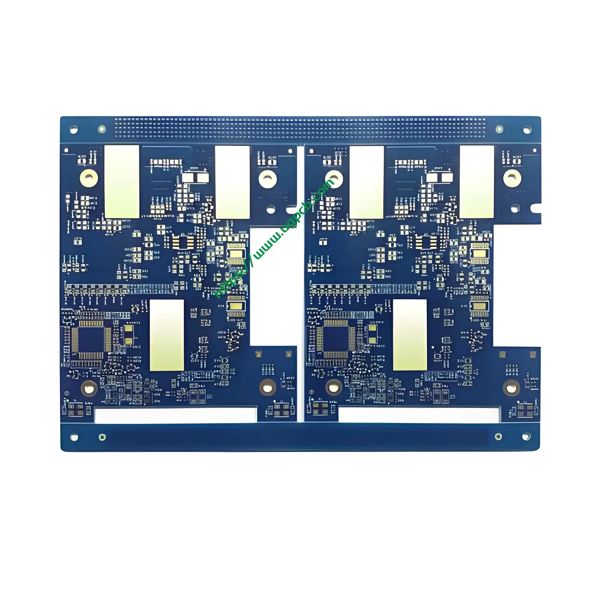
Constructed from FR-4 ITEQ, these PCBs offer excellent thermal stability and mechanical strength. The blue/white color scheme aids in visual inspection and troubleshooting. The finished thickness of 1.6mm provides a robust yet flexible board suitable for intricate designs.
構造と機能
The unique structure of a 12L 2+N+2 HDI PCB includes:
- Twelve Layers: Two core layers, n信号層, and another two core layers.
- High Density Interconnects: Allow for complex routing and minimal space usage.
- 表面処理: Immersion gold plus OSP enhances conductivity and protects against corrosion.
製造工程
The manufacturing process involves several sophisticated steps:
- 材料の準備: Selecting high-quality FR-4 substrate and copper foils.
- レイヤースタッキング: Arranging the layers in a precise order to achieve the desired “2+N+2” configuration.
- ボンディング: 熱と圧力を使用して層を結合します.
- エッチング: 余分な銅を除去するためにエッチャントを適用します, 目的の導電性経路のみを残します.
- メッキ: Adding a thin layer of metal to improve conductivity and solderability.
- 表面処理: Applying immersion gold plus OSP to protect against oxidation and enhance solderability.
- 品質管理: 各ボードが厳しい品質基準を満たすように徹底的な検査とテストを実施する.


ユースケースとシナリオ
12L 2+N+2 HDI PCBs are ideal for use in intelligent digital products where miniaturization and high performance are critical. 一般的なアプリケーションには含まれます:
- スマートフォン: 機能やパフォーマンスを損なうことなく、よりスリムなデザインを有効にします.
- タブレット: 高速データ転送と処理のための信頼できる接続を提供します.
- ウェアラブルデバイス: 堅牢なパフォーマンスと耐久性を維持しながら、コンパクトなデザインをサポートします.
- ポータブルメディアプレーヤー: 小さなフォームファクターで高品質のオーディオおよびビデオ処理機能を確保する.
結論は, the 12L 2+N+2 HDI PCB represents a pinnacle of innovation in PCB technology, 比類のない密度を提供します, パフォーマンス, 最も要求の厳しい消費者電子アプリケーションの信頼性.