
の概要 14 重い銅コイルPCBを重ねます
The 14 層の重い銅コイルPCBは高密度です, 堅牢な電気性能と信頼性を必要とするアプリケーション向けに設計されたマルチレイヤーパワーボード. これ プリント基板 高電力と信号の完全性を管理する必要がある複雑な電子システムに最適です.
何ですか 14 重い銅コイルPCBを重ねます?
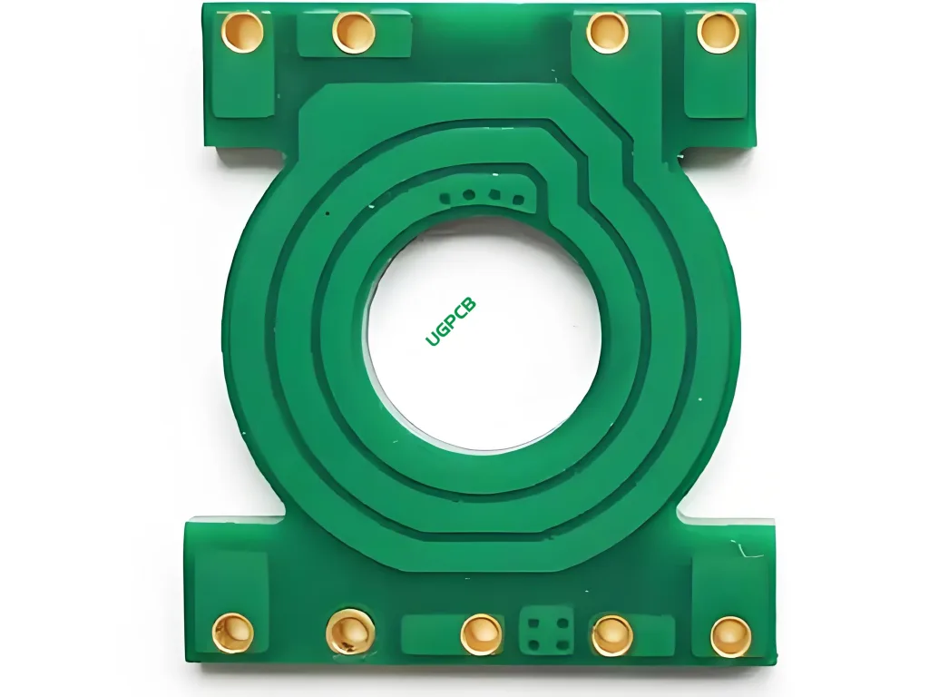
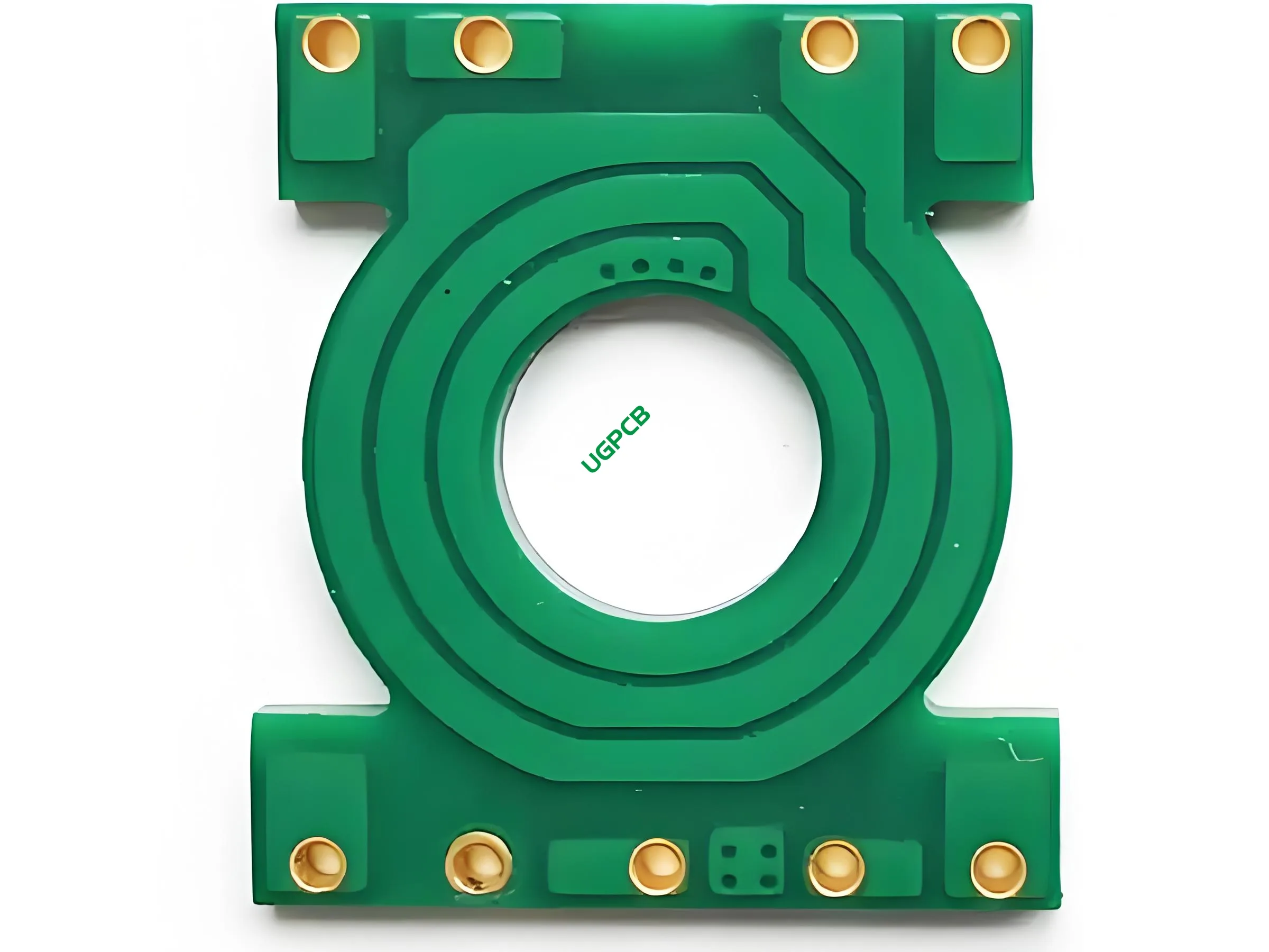
あ 14 層厚銅コイル PCB は、 プリント基板 (プリント基板) と 14 銅の痕跡の層, それぞれの計量 4 1平方フィートあたりのオンス. このタイプのPCBは、電源アプリケーション向けに特別に設計されています, 大きな電流を処理し、安定した電気接続を提供する必要がある場所.
設計要件
aの設計要件 14 重い銅コイルPCBを重ねて、そのパフォーマンスと信頼性を確保するために厳しい:
- 材料: EM827, 優れた電気および熱特性のために選択されます.
- レイヤー数: 14 複雑で密な回路設計に対応するためのレイヤー.
- 色: 簡単な識別と審美的な魅力のためのグリーン/ホワイト.
- 仕上がり厚さ: 4.0構造的完全性と耐久性を提供するMM.
- 銅の厚さ: 4適切な導電率と熱散逸を確保するためのOZ.
- 表面処理: はんだき性と腐食抵抗を高めるための浸漬金.
- 穴の銅の厚さ: 70より良い電気接続のために.
- 線幅: 0.3細かい回路パターンをサポートするMM.
- 最小開口: 0.4正確なコンポーネント配置を可能にするMM.
それはどのように機能しますか?
The 14 導電性経路を介して相互接続されるさまざまな電子コンポーネントを提供するためのプラットフォームを提供することにより、重い銅コイルPCB作業を層レイヤー. これらの経路, またはトレース, 銅で作られており、ボードにエッチングされています. 浸漬金表面処理は、これらの痕跡が導電性と環境要因に耐性のあるままであることを保証します.
アプリケーション
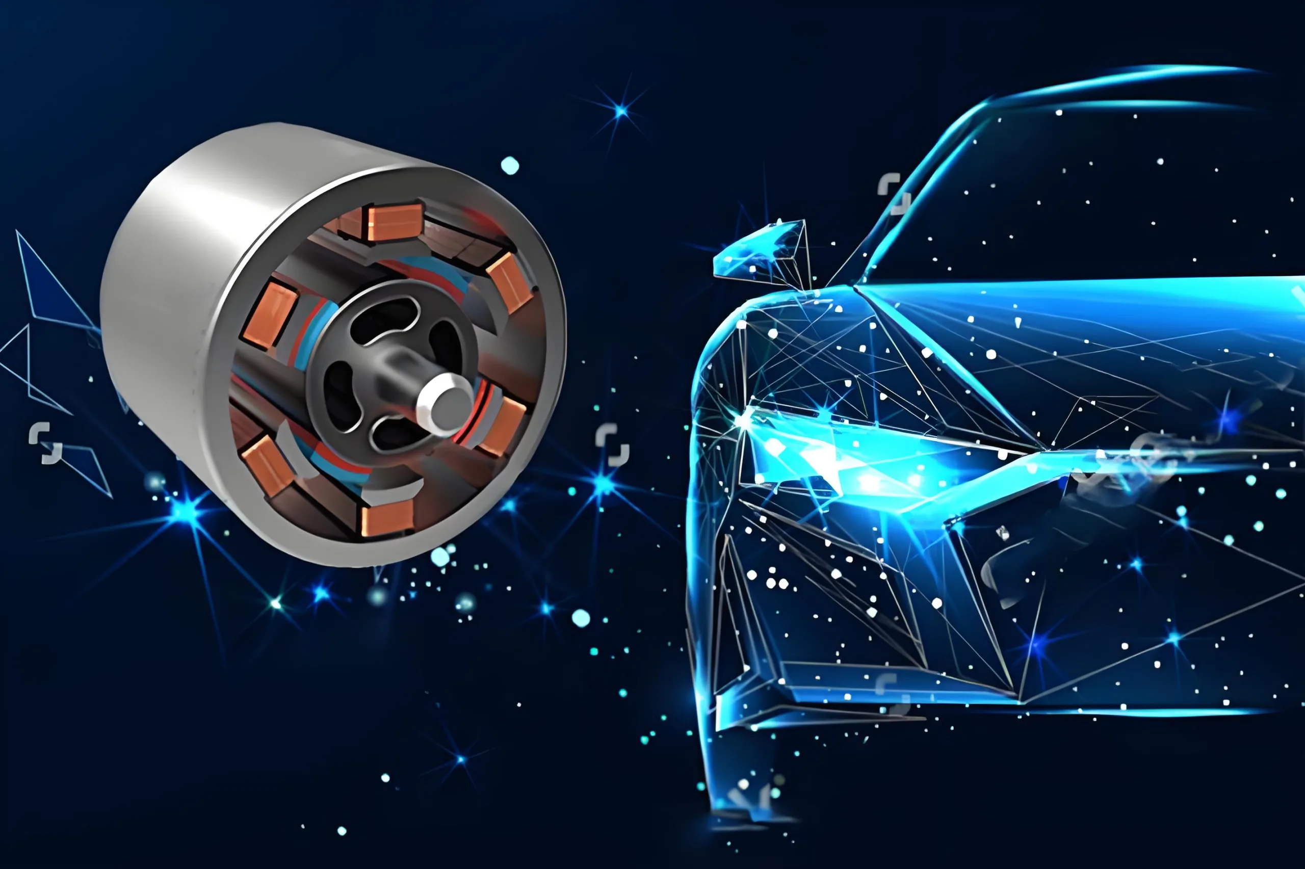
の主要なアプリケーション 14 重い銅コイルPCBは、電力の流れを管理および調節するパワーエレクトロニクスに含まれています. これには含まれます:
- 電源
- モータードライブ
- 再生可能エネルギーシステム
- 産業制御システム
分類
その機能とアプリケーションに基づいています, の 14 重い銅コイルPCBは、電力アプリケーションを要求するために設計された高電力PCBとして分類できます. この分類は、大きな電流を処理し、安定した電気接続を提供する能力を強調しています.
材料構成
コア 材料 で使用されます 14 重い銅コイルPCBはEM827です, 優れた機械式で知られている高性能ラミネート材料, サーマル, および電気的特性. この材料は、PCBが電力アプリケーションの需要に耐えることができることを保証します.
性能特性
のパフォーマンス特性 14 重い銅コイルPCBをレイヤーします:
- 高出力処理能力
- 優れた信号の完全性
- 優れた熱管理
- 堅牢な機械的強度
- 長期的な安定性
構造の詳細
の構造の詳細 14 層の重い銅コイルPCBは次のとおりです:
- レイヤー数: 14 レイヤー
- 仕上がり厚さ: 4.0mm
- 銅の厚さ: 4オズ
- 表面処理: イマージョンゴールド
- 穴の銅の厚さ: 701つ
- 線幅: 0.3mm
- 最小開口: 0.4mm
特徴と利点
の重要な機能と利点 14 重い銅コイルPCBをレイヤーします:
- 高密度相互接続性
- 優れた電力処理能力
- 堅牢な機械構造
- 信頼できる長期パフォーマンス
- 審美的な色のオプション (緑/白)
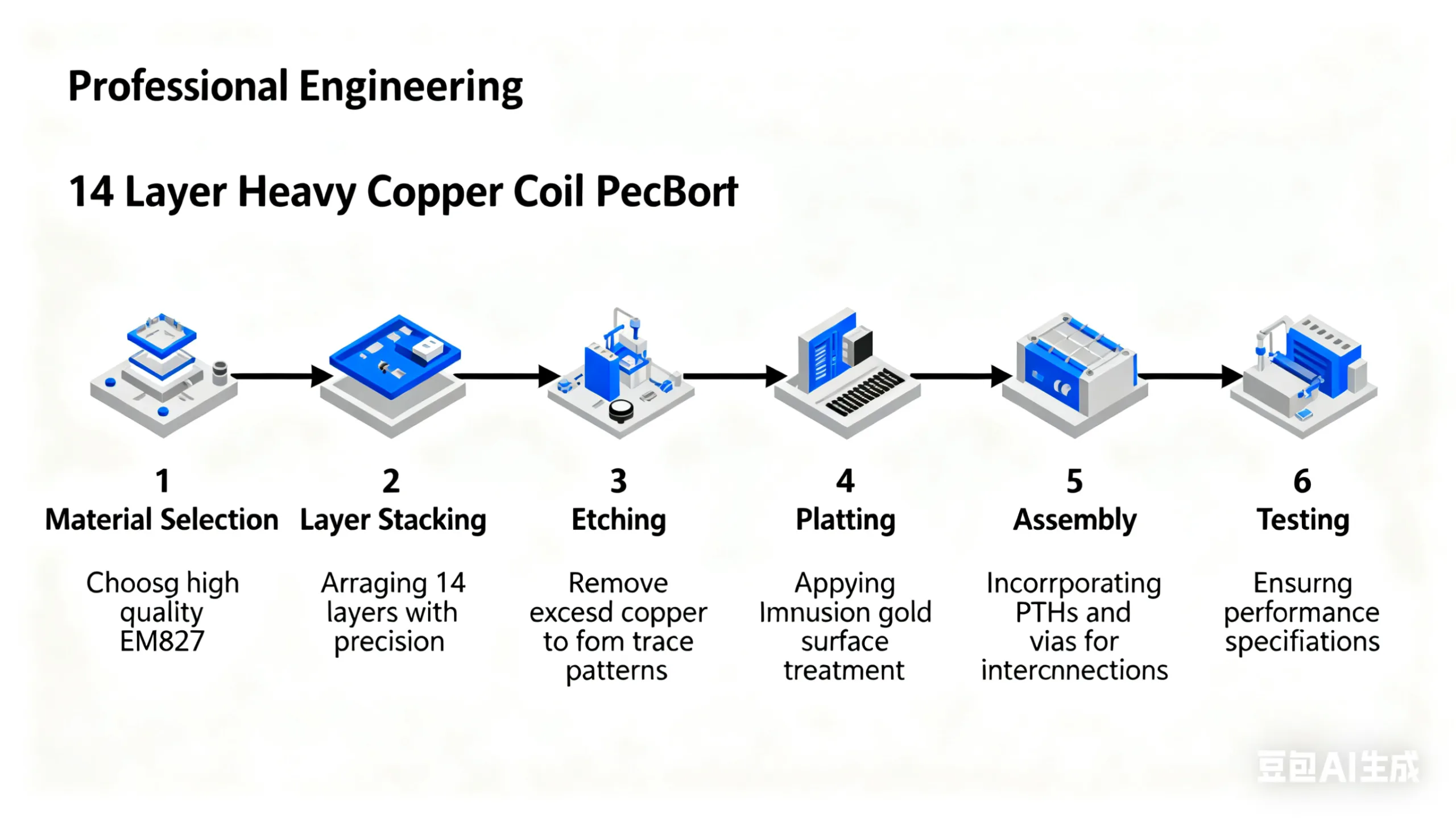
製造工程
の生産プロセス 14 重い銅コイルPCBを重ねるには、いくつかのステップが含まれます, 含む:
- 材料の選択: 高品質のEM827材料の選択.
- レイヤースタッキング: 配置 14 精度のあるレイヤー.
- エッチング: 過剰な銅を除去して、目的のトレースパターンを形成します.
- メッキ: 浸漬金表面処理の適用.
- 組み立て: 層相互接続にPTHとVIAを組み込む.
- テスト: PCBがすべてのパフォーマンス仕様を満たすようにします.
ユースケース
The 14 重い銅コイルPCBは、ようなさまざまなシナリオで使用されています:
- 高出力産業装置
- 再生可能エネルギーシステム
- モータードライブコントローラー
- 電源ユニット


