
UGPCB 18 層サーバー PCB: 高性能コンピューティング向けに設計 & データセンター
データセンターとクラウドコンピューティングの時代に, サーバーの安定性とパフォーマンスはデジタル ビジネスの運営にとって重要です. 基本的なハードウェアキャリアとして, サーバーの精密な設計と卓越した品質 プリント基板 (プリント基板) 最も重要です. 業界の深い専門知識と最先端のテクノロジーを活用, UGPCB 高いパフォーマンスを提供します, 次世代データセンター アプリケーションの最も厳しい要件を満たす信頼性の高い 18 層サーバー PCB.

製品の概要 & 意味
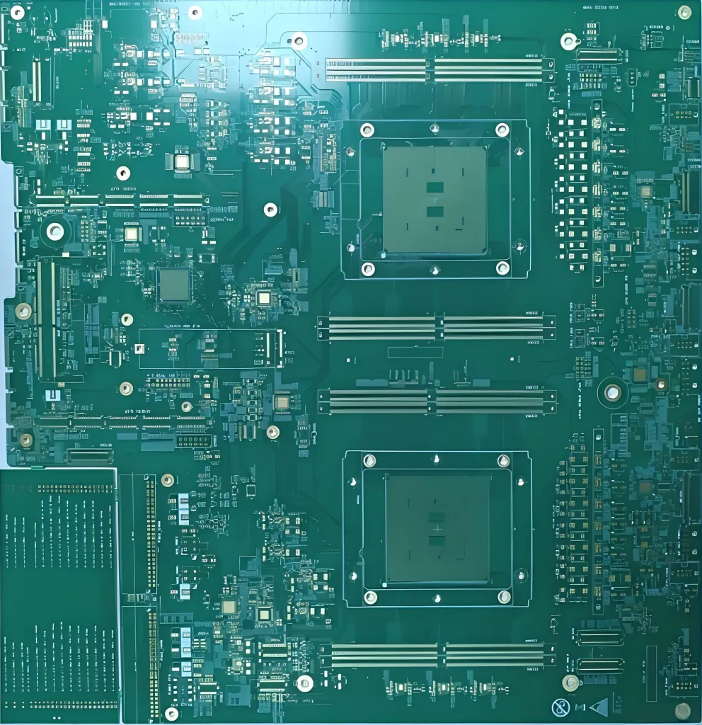
サーバー PCB はサーバー マザーボードのコア コンポーネントです, ストレージバックプレーン, およびさまざまな機能ドーターカード. CPUなどの重要なコンポーネントをホストします, メモリ, とチップセット, 高速信号伝送を容易にする, 配電, およびシステム相互接続. 高性能アプリケーションサーバー専用に設計, このUGPCB製品は18層の高多層構造を採用し、基板厚を2.4mm±10%に強化しました。, 大量のデータセットを処理し、高速計算をサポートするための堅牢なハードウェア基盤として機能します。.
コア設計のハイライト & テクニカル分析
サーバープラットフォームに対応するには’ シグナルインテグリティに対する極端な要求, パワーの完全性, および熱管理, この製品にはいくつかの主要なテクノロジーが統合されています:
-
高度なスタックアップ & 材料:
-
ラミネート: ITEQ IT968G高速を利用, 低損失材料. 高いTg (ガラス転移温度) 長期間の高温サーバー動作下でも寸法安定性と一貫した電気的性能を保証します。, 信号伝送ロスを効果的に低減.
-
レイヤー & 銅の重量: 綿密に設計されたハイブリッド銅重量スキームを備えた 18 層の複雑なスタックアップ (厳選された内層に2オンスの厚さの銅箔を採用). これにより、電源プレーンの通電容量と熱性能が最適化され、同時に高速信号層での細線配線が可能になります。.
-
-
精密な配線 & 相互接続:
-
回線能力: 線幅/スペース0.1mm/0.1mmの超細線を実現, 高密度 BGA パッケージのファンアウトおよび相互接続要件を満たす (例えば。, CPU, GPU, FPGA).
-
Microviaテクノロジー: 最小直径 0.20mm の機械ドリルをサポート, 配線密度とスペース利用率の向上.
-
-
シグナルインテグリティのための主要なテクノロジー:
-
バックドリリング: 高速差動信号用 (例えば。, PCIE, SAS, イーサネット), バックドリルプロセスにより、スルーホールから未使用の銅スタブが除去されます。, 信号の反射と減衰を大幅に低減. これは、信号品質を確保するための中心的なプロセスです。 高速PCB.
-
RTF銅箔: 逆処理箔を使用, より滑らかな銅表面を提供します. これにより、高周波信号の表皮効果損失が効果的に低減されます。, 信号伝送効率の向上.
-
-
信頼性の高い表面仕上げ:
-
エレクトロレスニッケルイマージョンゴールド (同意する) 最終表面処理として施されます. ENIG は平らな表面を提供します, 優れたはんだ付け性, 信頼性の高い接触インターフェース, 長期的な耐酸化性, 緻密なはんだ付けに最適です, ファインピッチ コンポーネント サーバー PCB 上.
-
製品の特徴 & 利点
-
優れた電気的性能: 高速 IT968G ラミネートとバックドリリングおよび RTF フォイルの組み合わせにより、低損失を実現, 高周波信号の低遅延伝送, にとって理想的な選択肢となります 高周波プリント基板 そして 高速PCB.
-
優れたパワーハンドリング & 熱管理: 2Oz の内層銅と 2.4 mm 基板設計により、通電容量が向上, 全体的な構造剛性, と熱伝導率.
-
高密度 & 信頼性: 18 層の配線スペースと 0.1/0.1 mm の線幅/スペースが最も複雑なデザインをサポートします. 厳格なプロセス制御と高 Tg 材料により、製品の長期信頼性が保証されます。 24/7 中断のない動作.
-
エンドツーエンドのサービスサポート: UGPCB はトップティアだけを提供するだけではありません プリント基板の製造 デザインレビューから生産までのワンストップソリューションも提供します, 市場投入までの時間を短縮する.
製造工程の概要
当社の製造は厳格な基準を遵守しています IPC標準 品質管理システム:
エンジニアリングレビュー → 材料準備 → 内層イメージング → ラミネート → 穴あけ & バックドリリング → ホールメタライゼーション → 外層イメージング → メッキ (ハイブリッド銅重量用) → ソルダーマスク塗布 (Pre-ONE) → ENIG → ルーティング / プロファイリング→電気テスト & 最終検査
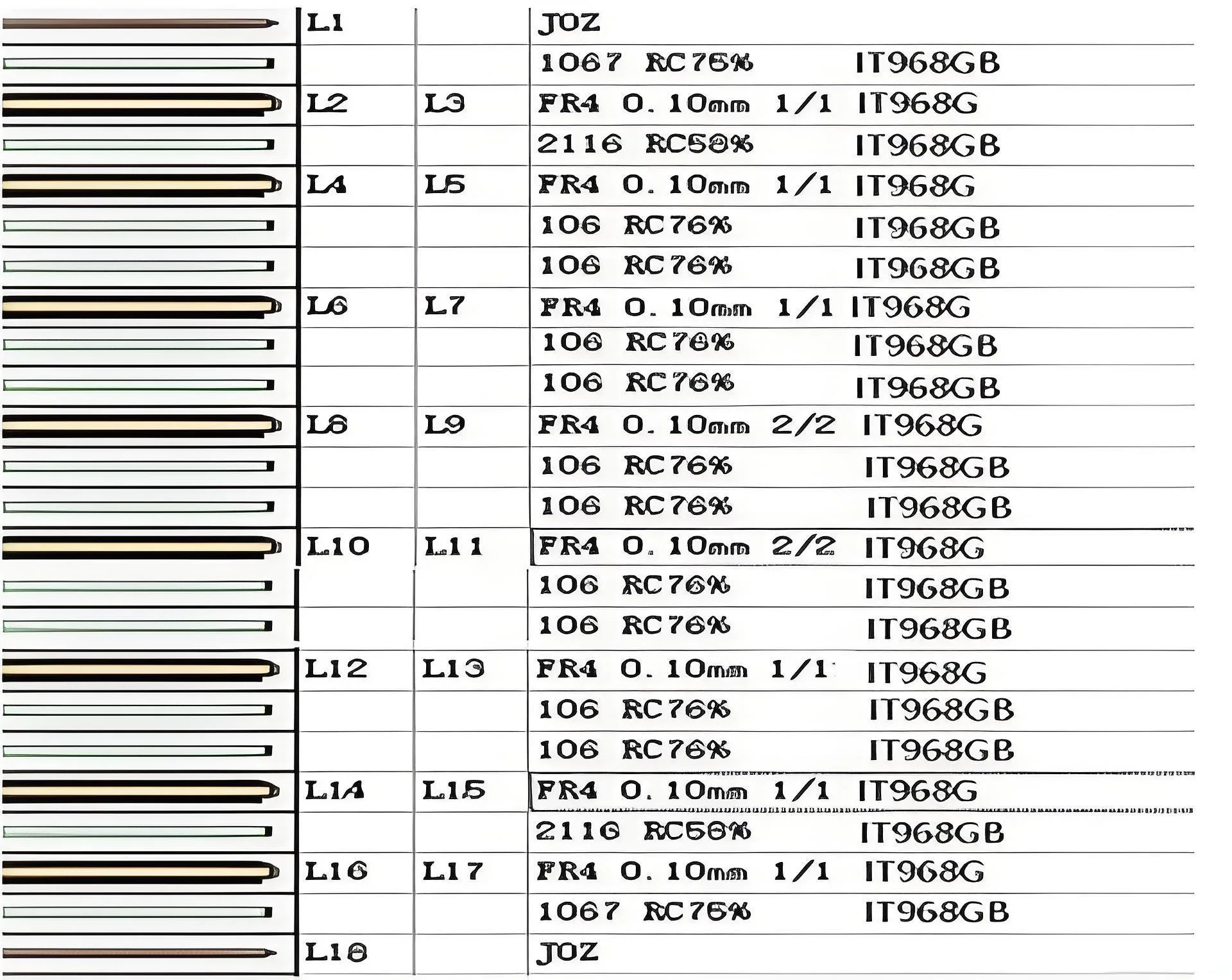
https://via.placeholder.com/800×450.png?text=18層+PCB+断面図
代替テキスト: 18層サーバーPCB基板の断面図, 高速信号伝送のための精密な積層とバックドリルビア構造の詳細.
アプリケーション & 分類
この高性能PCBは、さまざまな分野で広く使用されています。:
-
企業 & クラウドサーバーのマザーボード
-
データセンター AI コンピューティング アクセラレーション カード
-
高性能ストレージサーバー & バックプレーン
-
ネットワークスイッチ & 通信機器コアボード
技術分類:
-
レイヤーカウントごとに: 高い 多層プリント基板 (18 レイヤー)
-
テクノロジーによって: 高速・高周波基板, バックドリルPCB, 重い銅の PCB
-
アプリケーションによって: サーバー/データセンター PCB
-
表面仕上げによる: 同意する (エレクトロレスニッケルイマージョンゴールド) プリント基板
UGPCBを選択します, 高品質のサーバー PCB ボードだけではありません。; 高度な PCB 製造において信頼できるパートナーを獲得できます. 私たちは、複雑な技術的詳細をお客様の製品の信頼できる利点に変換することに専念しています。, 次世代のデータセンター ソリューションを強化.
カスタマイズされた PCB ソリューションの見積もりと技術的な相談については、今すぐ当社の専門家チームにお問い合わせください。!


