
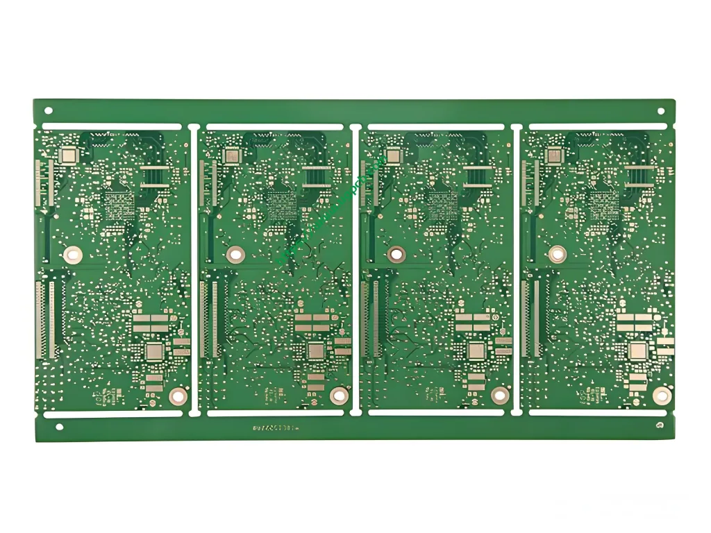
UGPCBの8層1+N+1 HDI PCB: 包括的なガイド
エレクトロニクスの小型化と高性能化のあくなき追求, 高密度相互接続 (HDI) プリント基板 礎石となった. UGPCB の 8 レイヤー 1+N+1 HDI 製品は、可能性の限界を押し上げる設計者のための洗練されたソリューションを表します. この記事では、この高度な機能について詳しく説明します。 プリント基板 テクノロジー.
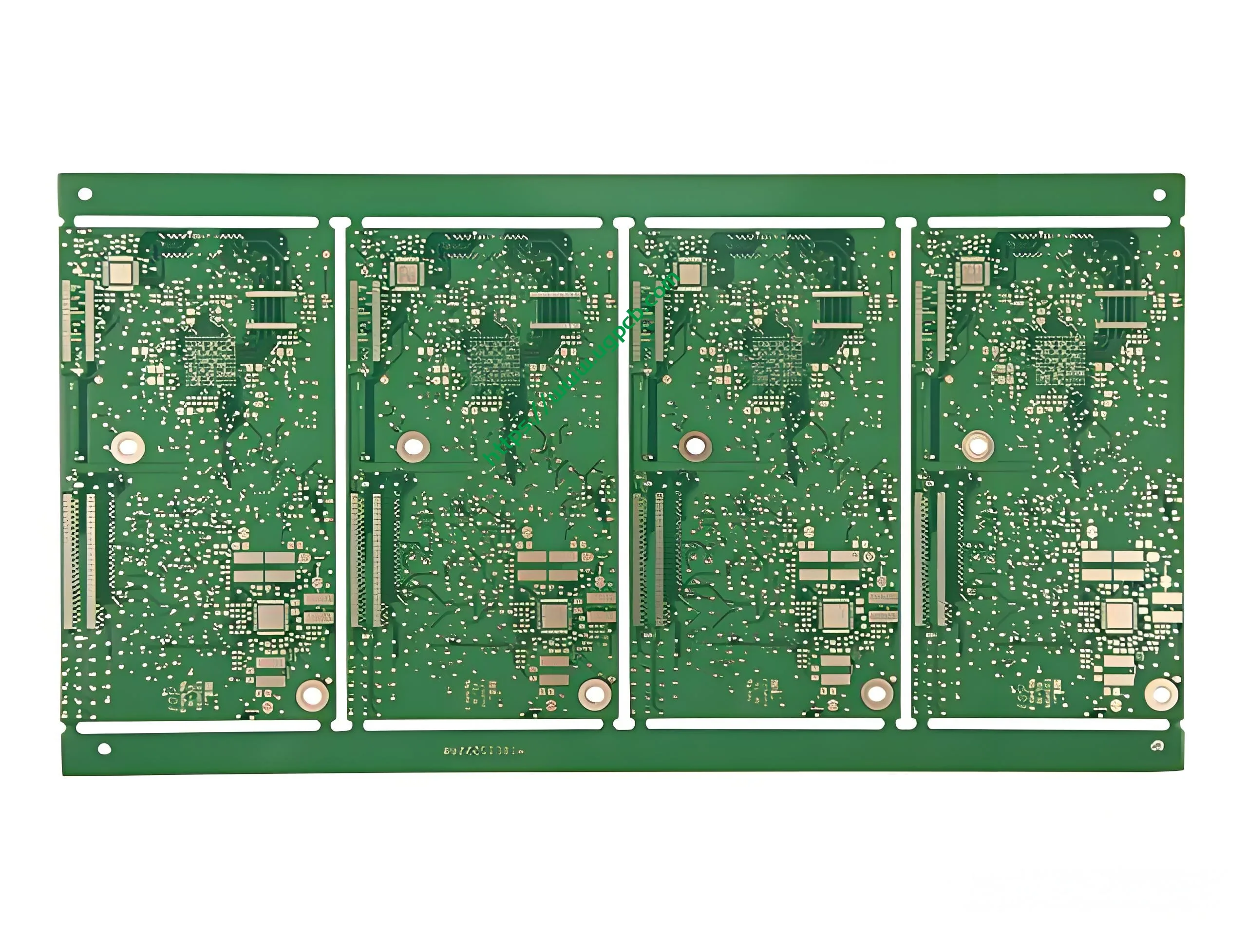
8 層 1+N+1 HDI PCB とは?
8 層 1+N+1 HDI PCB は、特定のタイプの 高密度相互接続ボード. 命名法 “1+n+1” マイクロビアのビルドアップ構造を説明します.
-
最初と最後の「1」: これらは、基板の上面と底面にある単一層の高密度マイクロビアを表します。. これらのマイクロビアは通常、レーザー穴あけ加工を使用して作成されます.
-
それから': これはボードのコアを表します, この場合は標準の 6 層です 多層PCB (合計を作る 8 レイヤー). コアには、内部層を接続するスルーホールまたは埋め込みビアが含まれています.
この構造により、コンパクトなスペースで非常に多くの相互接続が可能になります。, コンプレックスに最適です, スペースに制約のある PCBデザイン 現代のマイクロエレクトロニクス製品には不可欠.
主な設計上の特徴と仕様
UGPCB はこの HDI PCB を精密に製造しています, 次の重要な仕様を遵守する:
-
材料: 高Tg FR-4, 優れた熱的および機械的安定性を提供する堅牢で信頼性の高いラミネート.
-
板厚: 仕上がり厚さ0.8mm, スリムな製品プロファイルをサポート.
-
銅の重量: 1 オンス (35μm) インナーレイヤー用と 0.5 オンス (17.5μm) 外層用. このバランスにより、良好な電流容量が保証されると同時に、より微細な外層トレースのエッチングが可能になります。.
-
表面仕上げ: イマージョンゴールド (同意する) OSP経由で (有機はんだ付け性防腐剤) 財団. この組み合わせによりフラットになります。, はんだ付け用の耐久性のある表面と優れた保存寿命.
-
最小トレース/スペース: 3 ミル (0.075 mm), 高密度回路を可能にする.
-
最小穴サイズ: 0.2機械ドリルの場合は mm、レーザーで穴開けされたマイクロビアの場合は超微細 0.1 mm.
この HDI PCB 構造の仕組み
The “1+n+1” より効率的なルーティング経路を作成することでアーキテクチャが機能します. すべての層で貴重な不動産を消費する大きなスルーホールを使用する代わりに, これ HDI PCB 設計 マイクロビアを利用. レーザーで開けられたこれらの小さな穴は、隣接する層のみを接続します。 (例えば。, L1~L2, またはL8~L7). これ “積み重ねられた” または “千鳥状” via アプローチにより、内層のルーティング チャネルが解放されます, コンポーネント密度が大幅に向上し、信号パスがより効率的になります。, これは高速化にとって重要です PCBAアセンブリ.
主なアプリケーションとユースケース
この高度な HDI PCB の主な用途は、洗練されたマイクロエレクトロニクス製品です。. 具体的な使用例としては、:
-
ウェアラブルテクノロジー: スマートウォッチ, フィットネストラッカー, および医療用モニター.
-
先進的なモバイルデバイス: スマートフォン, 錠剤, ウルトラポータブルラップトップ.
-
高密度医療機器: 小型の医用画像診断装置.
-
航空宇宙および防衛航空電子工学: 信頼性とサイズが最優先される場合.
素材構成: FR-4ラミネート
FR-4 材料の選択は戦略的です. 優れたパフォーマンスバランスを提供します, 料金, と製造性. この 0.8mm 厚の HDI PCB の場合, ガラス転移温度が高いハイグレードFR-4 (TG) 複数のラミネートサイクルによる熱ストレスに耐えるために使用され、鉛フリーです。 プリント基板 はんだ付け工程.
性能と構造上の利点
1+N+1 HDI ボードの構造は、パフォーマンスの大幅な向上に直接つながります。:
-
信号の整合性の向上: 相互接続パスが短いため、信号損失と伝播遅延が減少します。.
-
改善された熱管理: 高密度ビア構造により熱放散が促進されます。.
-
優れた信頼性: マイクロビアの使用により、熱サイクル中のはんだ接合部の破損のリスクが軽減されます。.
-
サイズと重量の削減: HDI テクノロジーの核となる利点, より小型の最終製品を可能にする.
製造プロセスの簡略化された概要
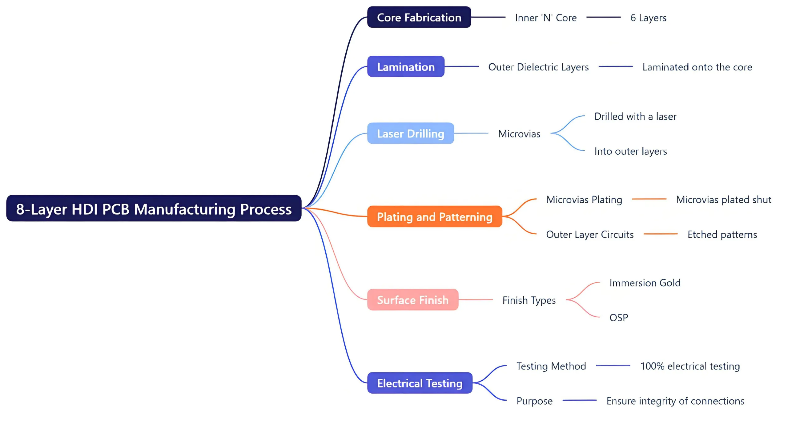
この HDI PCB の製造は複数のステップから成ります。, 精密加工:
-
コアの製造: 内なる「N」’ コア (6 レイヤー) 最初に生産される.
-
ラミネート加工: 外側の誘電体層はコア上に積層されます.
-
レーザー穴あけ加工: マイクロビアはレーザーで外層に穴を開けられます.
-
メッキとパターニング: マイクロビアはメッキで閉じられています, 外層回路をエッチング.
-
表面仕上げ: イマージョン ゴールドと OSP が適用されます.
-
電気テスト: 100% 電気テストによりすべての接続の完全性が保証されます.
HDI PCB および PCBA のニーズに UGPCB を選択する理由?
8 層 HDI PCB 製造における UGPCB の専門知識は、プロジェクトに明確な利点をもたらします. 基板を確実に生産する能力 3/3 ミルラインと0.1mmマイクロビアにより、複雑なPCB製造のリーダーとしての地位を確立. これにより、彼らは理想的なパートナーとなるだけでなく、 PCB製造 完全なターンキー PCBA サービスにも対応, 設計から完成品までシームレスに移行できるようにする, 組立品.


