
の紹介 24 通信バックプレーンPCBをレイヤーします
The 24 レイヤー通信バックプレーンPCBは高性能です プリント基板 複雑な通信システム用に設計されています. 堅牢な接続と信頼性の高い信号伝送を提供するように設計されています, 高度な通信アプリケーションに最適です.
何ですか 24 通信バックプレーンPCBをレイヤーします?
あ 24 レイヤー通信バックプレーンPCBは、を指します 多層プリント回路基板 それは特別に設計されています 24 誘電層によって分離された導電性材料の層. この構造により、信号の完全性を維持し、干渉を最小限に抑えながら、高密度相互接続性が可能になります.
設計要件
aの設計要件 24 レイヤー通信バックプレーンPCBは、重要な通信システムに適用されるため、厳格です. 主要な設計上の考慮事項には含まれます:
- 材料: パナソニックM6, 優れた熱および電気特性で知られています.
- レイヤー数: 24 複雑なルーティングのニーズに対応するためのレイヤー.
- 色: 簡単に識別と美的魅力のための青/白.
- 仕上がり厚さ: 2.0過度にかさばらずに構造的完全性を確保するためのmm.
- 銅の厚さ: 1適切な導電率を提供するOZ.
- 表面処理: はんだき性と腐食抵抗を高めるための浸漬金.
それはどのように機能しますか?
The 24 レイヤー通信バックプレーンPCBは、誘電材料で分離された複数の層の銅の痕跡を使用して動作します. これらのレイヤーは、メッキされたスルーホールを介して相互接続されています (pths) またはVIAS, 異なるレイヤー間を移動できるように信号を許可します. 浸漬金表面処理は、銅の痕跡が導電性と酸化に耐性のあるままであることを保証します.
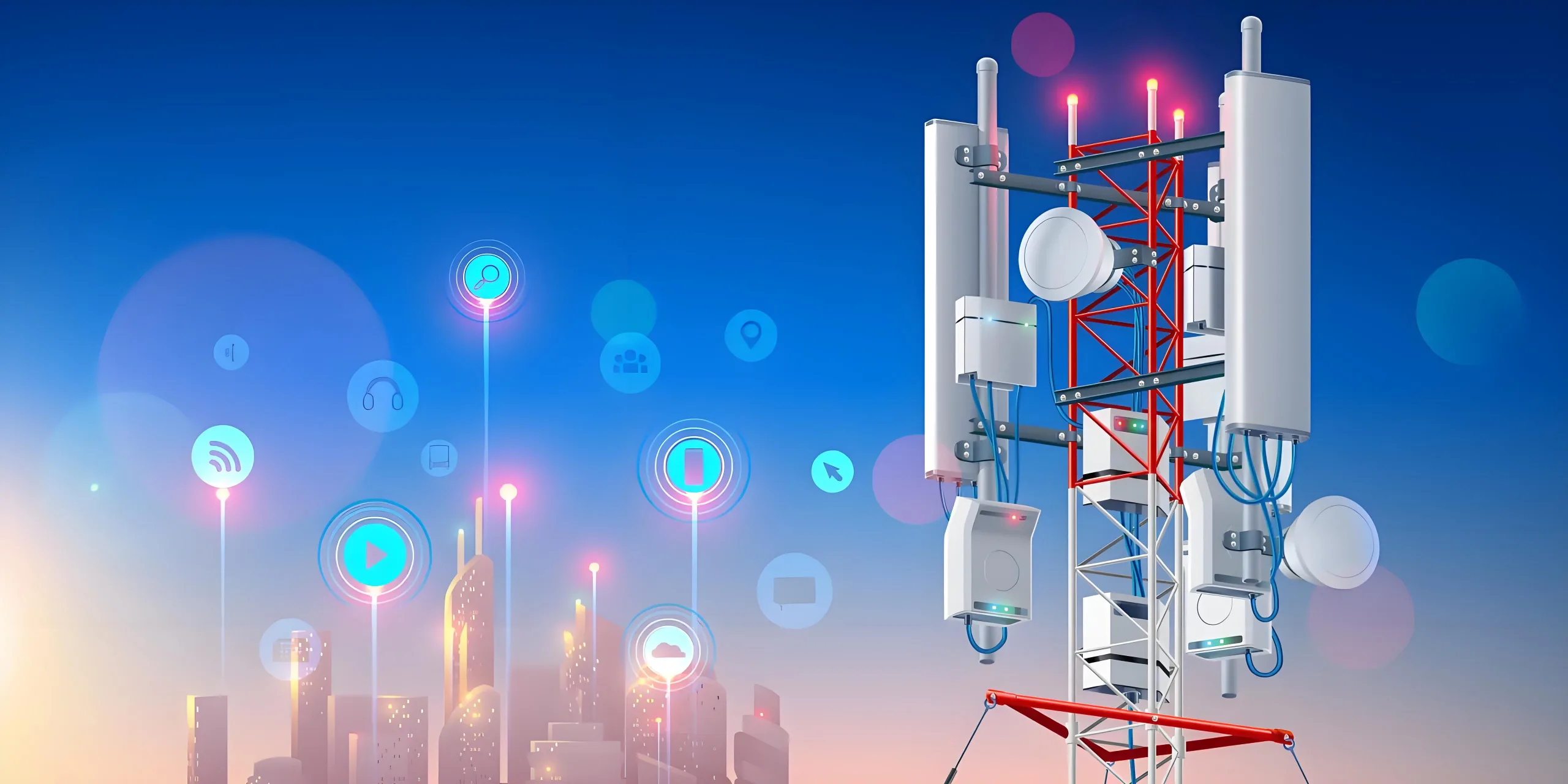
アプリケーション
の主要なアプリケーション 24 レイヤー通信バックプレーンPCBは、高速データ送信と信頼できる接続が非常に重要な通信バックプレーンにあります. これら プリント基板 で使用されます:
- テレコムインフラストラクチャ
- データセンター
- 高周波通信デバイス
- ネットワーキング機器
分類
その機能とアプリケーションに基づいています, の 24 レイヤー通信バックプレーンPCBは、ハイマルチライヤーPCBに分類できます. この分類は、最新の通信システムに必要な複雑で密な回路設計を処理する能力を強調しています.
材料構成
コア 材料 で使用されます 24 レイヤー通信バックプレーンPCBはパナソニックM6です, 優れた機械式で知られている高性能ラミネート材料, サーマル, および電気的特性. この資料は、PCBが高速通信アプリケーションの要求に耐えることができることを保証します.
性能特性
のパフォーマンス特性 24 レイヤー通信バックプレーンPCBが含まれます:
- 高い信号の完全性
- 低信号損失
- 優れた熱管理
- 機械的強度の向上
- 信頼できる長期安定性
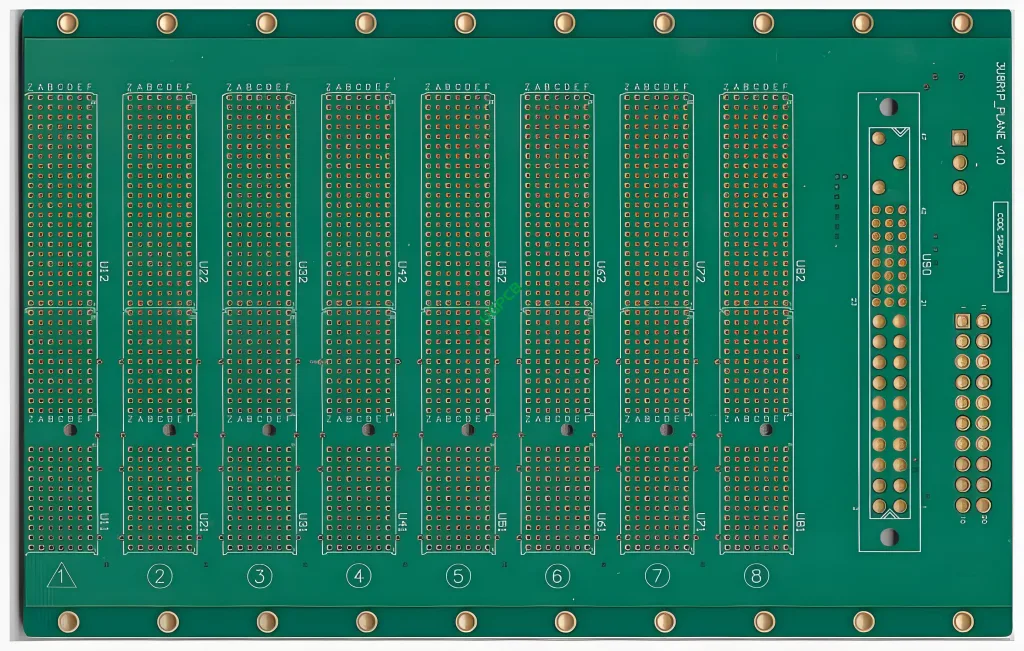
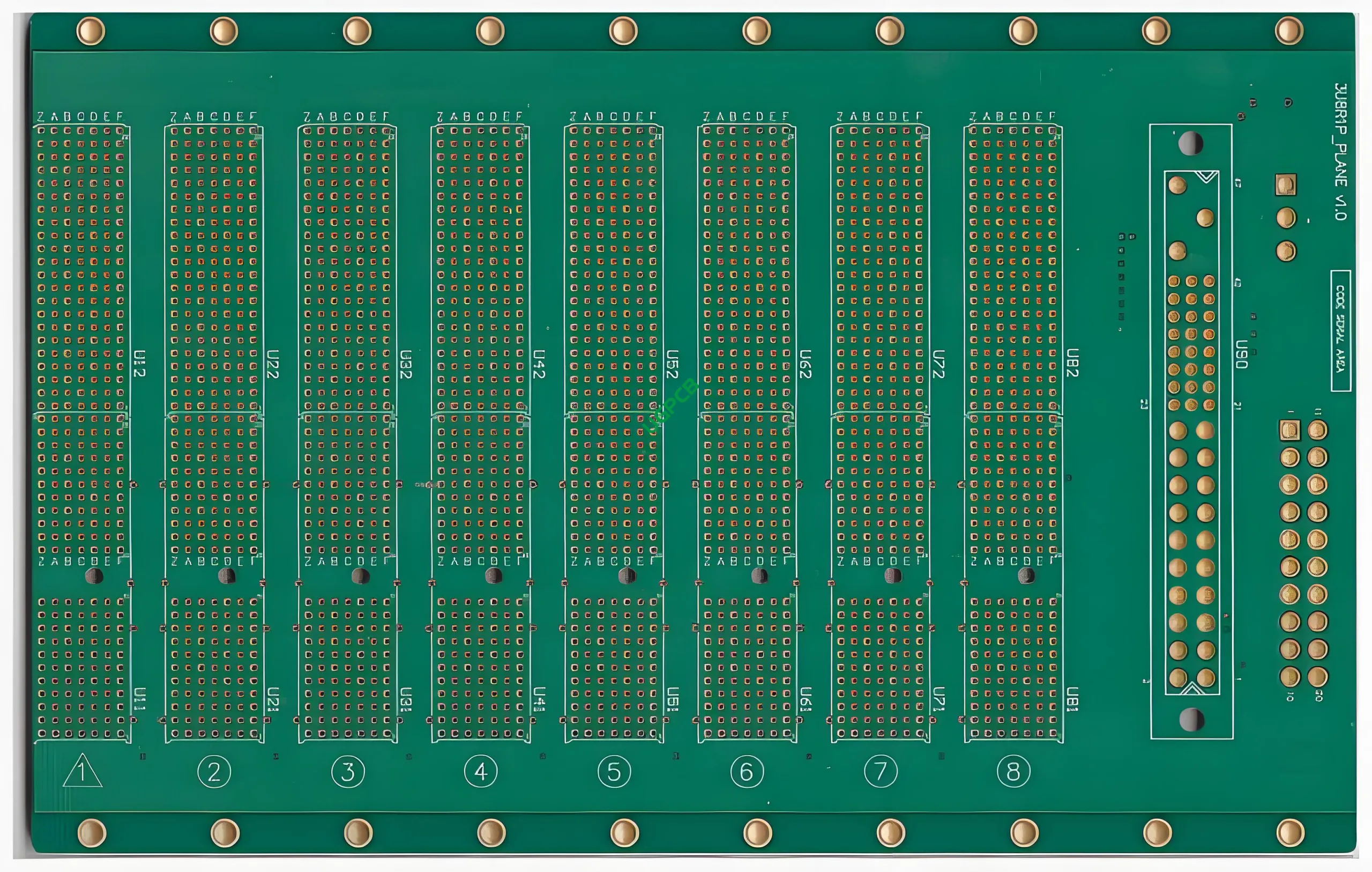
構造の詳細
の構造の詳細 24 レイヤー通信バックプレーンPCBは次のとおりです:
- レイヤー数: 24 レイヤー
- 仕上がり厚さ: 2.0mm
- 銅の厚さ: 1オズ
- 最小トレース幅: 6ミル (0.15mm)
- トレース間の最小スペース: 6ミル (0.15mm)
- 表面処理: イマージョンゴールド
特徴と利点
の重要な機能と利点 24 レイヤー通信バックプレーンPCBが含まれます:
- 高密度相互接続性
- 優れた信号の完全性
- 堅牢な機械構造
- 信頼できる長期パフォーマンス
- 審美的な色のオプション (ブルー/ホワイト)
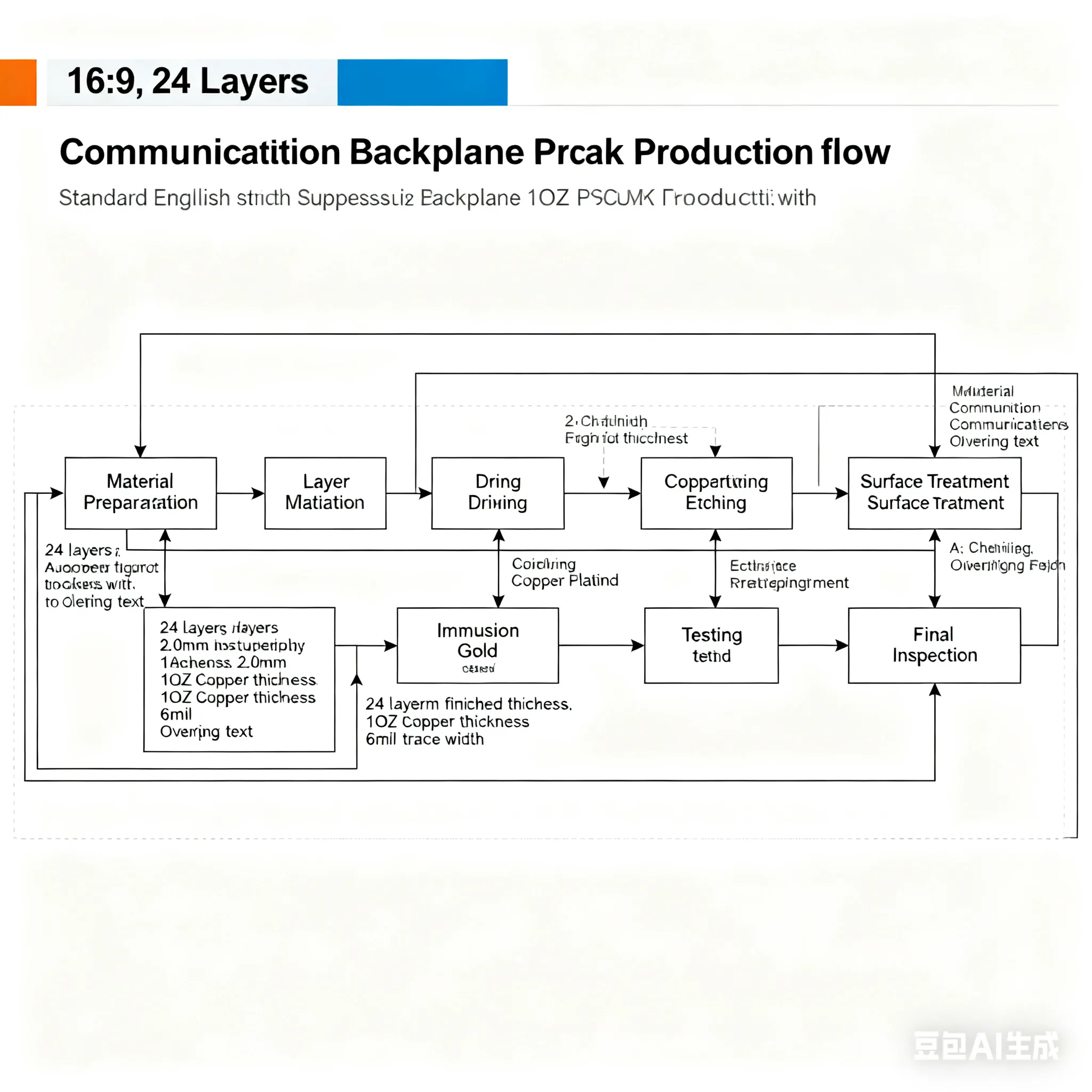
製造工程
の生産プロセス 24 レイヤー通信バックプレーンPCBにはいくつかのステップが含まれます, 含む:
- 材料の選択: 高品質のパナソニックM6材料の選択.
- レイヤースタッキング: 配置 24 精度のあるレイヤー.
- エッチング: 過剰な銅を除去して、目的のトレースパターンを形成します.
- メッキ: 浸漬金表面処理の適用.
- 組み立て: 層相互接続にPTHとVIAを組み込む.
- テスト: PCBがすべてのパフォーマンス仕様を満たすようにします.
ユースケース
The 24 レイヤー通信バックプレーンPCBは、さまざまなシナリオで使用されます, のような:
- 高速データ送信ネットワーク
- 通信インフラストラクチャプロジェクト
- 高度なネットワーキング機器
- 高い帯域幅を必要とするデータセンターアプリケーション
要約すれば, の 24 レイヤー通信バックプレーンPCBは、最新の通信システムの厳しい要件を満たすように設計された洗練された信頼性の高いコンポーネントです. その高密度設計, 優れたパフォーマンス特性, 堅牢な構造により、高度な通信セットアップの重要な部分になります.


