UGPCB 26 層高性能サーバー PCB: データセンターのコンピューティング能力の中核基盤
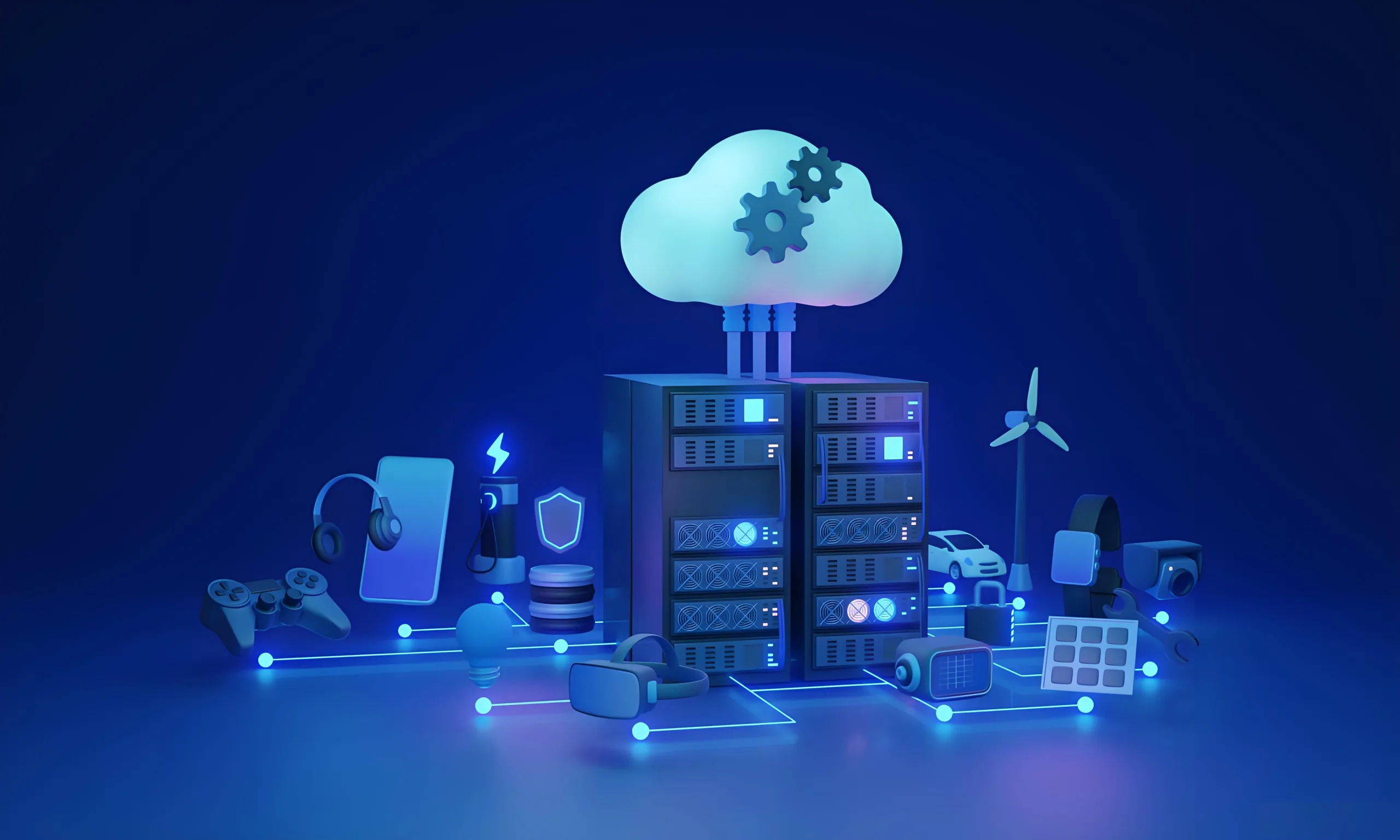
デジタル時代に, サーバーは “超頭脳” 大量のデータを処理する, そして サーバ プリント基板 (プリント基板) 重要です “ニューラルネットワーク” この脳の. うまく設計された, 精密に製造されたハイエンド サーバーのマザーボードPCB データセンターの処理速度を直接決定します, 電力効率, 長期にわたる動作安定性. 深い専門知識を活用して、 高速, 高層カウント プリント基板の製造, UGPCB がこのフラッグシップを開発しました 26-レイヤサーバーPCB 次世代ハイパフォーマンスコンピューティングに向けて (HPC), AIサーバー, およびクラウドデータセンター. 卓越した電気的性能と信頼性の高い物理構造を提供し、極端な計算負荷をサポートするように設計されています。.
製品の定義 & 概要: ハイエンドサーバーPCBとは?
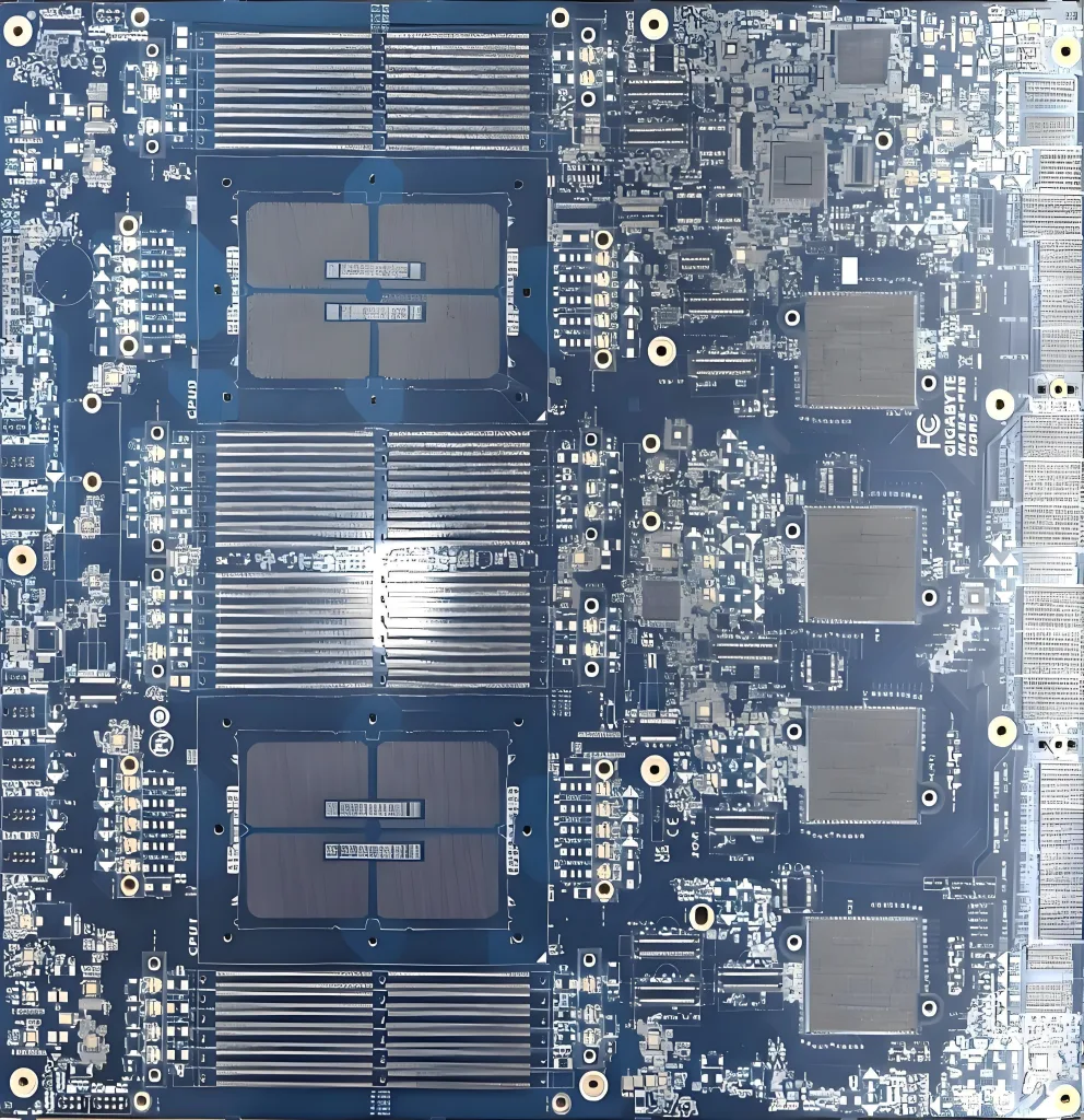
ハイエンドサーバーの PCB は複雑です, CPUなどのコアコンポーネントをホストするように設計された多層回路基板, メモリ, 高速インターフェース (例えば。, PCIE, CXL), および電源管理ユニット, 超高速を確立するために, それらの間の電気的接続の信頼性が高い. これは単なる機械基板ではなく、GHz 周波数での信号の完全性と電力の完全性を確保するための重要なプラットフォームです。. これ UGPCB 製品の特徴は洗練された 26-層PCBスタックアップ, ビッグデータ処理や AI トレーニングなどの要求の厳しいアプリケーション向けに特別に設計された高度な素材とプロセスを利用します.
コア設計ポイント & 作業原則
サーバー PCB の主な機能は、低損失を提供することです。, 高速デジタル信号と大電流電力供給のための低干渉伝送パス. その設計はいくつかの重要な原則を中心に展開されています:
-
信号の完全性 (そして): の使用 高速材料 (TG 170) と正確な制御 トレース幅/間隔 0.08mm/0.09mm 信号の減衰と歪みを最小限に抑えます, 数十Gb/秒の速度でエラーのないデータ伝送を保証.
-
パワーの完全性 (PI): の組み込み 2オンスの重銅 (2/2 オンス) 電源プレーンと内部プレーンの DC 抵抗と温度上昇を低減, CPU/GPUなどの高出力チップに十分でクリーンな電力を供給します。.
-
インピーダンス制御 & バックドリリング: 高速チャンネルには厳密なインピーダンス制御が適用されます. 重要なイノベーションは、 バックドリリング技術 未使用の導電性スタブを削除するには (バレル) メッキスルーホールの, 信号反射点の除去 - 信号の反射点を改善するための中心的なプロセス の信号品質 高速PCB.
-
熱管理 & 信頼性: あ 完成板厚 2.97mm ±10% そして 高いTg 170 材料 優れた機械的強度と耐熱性を提供します, 長期間の環境下でも PCB の安定性と信頼性を確保します。, 高温, サーバーのフルロード動作.
技術仕様 & 材料
-
レイヤー数 & 厚さ: 26 レイヤー, 仕上がり板厚 2.97mm±10%.
-
銅の重量の積み重ね: 複雑な構成: 1/1/H/1/H/1/H/1/H/1/H/2//2/2/H/1/H/1/H/1/H/1/H/1/1オンス. クリティカルな電力層の使用 2オンスの重銅 信号と電力のニーズのバランスを取る.
-
コア素材: タイヤオ TU883 高速, 低損失ラミネート と ガラス転移温度 (TG) 170℃以上. 非常に低い誘電率を実現します (DK) および散逸率 (Df), にとって最高の選択肢となります 高速PCB材料.
-
線の精度: 最小トレース幅/スペース 0.08mm / 0.09mm, 高密度配線を可能にする.
-
マイクロビア技術: をサポートします。 最小機械ドリル直径 0.20mm, 高密度相互接続に対応 (HDI) 要件.
-
表面仕上げ: 有機はんだ付け性防腐剤 (OSP) アパートを提供します, 高性能BGAおよびチップ向けのはんだ付け性の高い表面 コンポーネント, 優れたコストパフォーマンスを実現.
製品分類, 構造 & 特徴
-
科学的分類: この商品は以下のカテゴリーに属します “ハイエンド多層高速サーバーマザーボード PCB”, 具体的には “高Tg, 多層レイヤー数, バックドライル, 厚銅の電力供給 PCB”.
-
主要な構造的特徴:
-
多層ラミネート: 信号の正確な配置, 地面, および電源プレーンは、効果的な電磁シールドと低インピーダンスのリターンパスを作成します。.
-
バックドリル構造: 重要な高速リンク用のスルーホール (例えば。, PCIeレーン, メモリスロットの接続) 高周波性能を大幅に向上させるためにバックドリル加工が施されています.
-
RTF銅箔塗布: 逆処理箔の使用により、より滑らかな銅表面が得られます。, 導体に沿った伝送中の信号損失をさらに低減します。.
-
厳格な製造プロセス
UGPCB の製造プロセスは IPC-A-600G/6012 クラスに厳密に準拠しています 2/3 標準, サーバー PCB の制御を強化:
材料切断 → 内層イメージング & AOI検査→ラミネート & 穴あけ加工 → 無電解 & 電解銅堆積 → バックドリルプロセス → 外層イメージング → 二次 AOI & インピーダンステスト → ソルダーマスク & OSP アプリケーション → 電気テスト (フライングプローブ/テストフィクスチャ) → 最終目視検査 & 包装.
このうち, バックドリリング そして インピーダンス試験 この品質を保証する重要な管理ポイントです 高性能サーバーPCB.
対象アプリケーション
この製品は、以下のハイエンドアプリケーション向けに特別に設計および製造されています。:
-
人工知能 & 機械学習サーバー: トレーニングおよび推論 GPU/ASIC クラスターのホスティング.
-
クラウドコンピューティング & データセンターサーバー: ハイパフォーマンスコンピューティング向け (HPC) クラスターと仮想化ホスト.
-
エンタープライズストレージサーバー: 高い信頼性と多数の高速データインターフェースを必要とするストレージデバイス.
-
5Gコアネットワーク機器: 高速データスイッチングに対応したネットワークインフラ.