
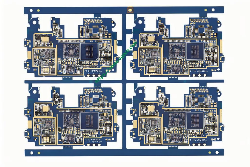
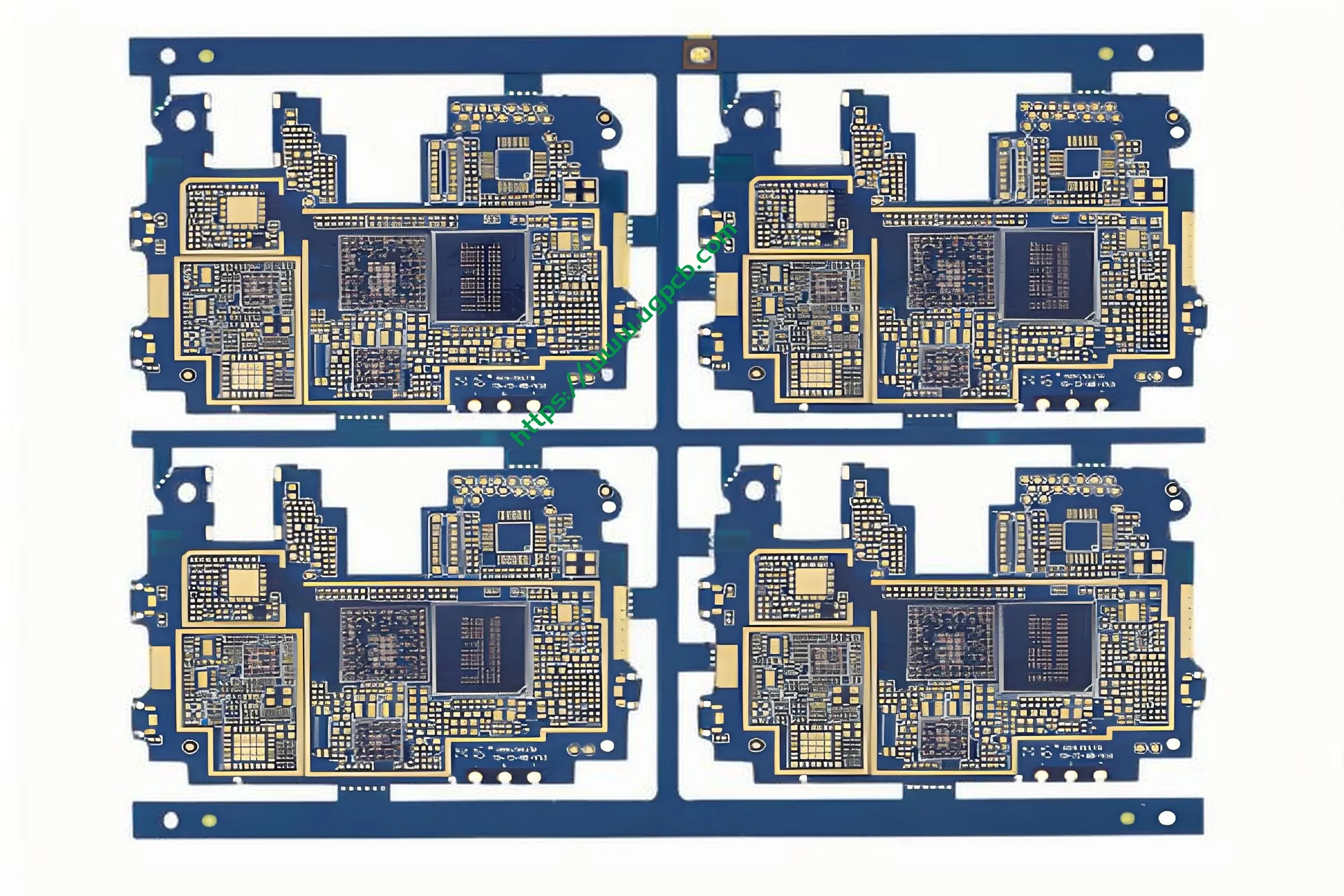
Overview of 8Layers 2+N+2 HDI PCB
The 8Layers 2+N+2 HDI PCB is a high – density interconnect プリント基板. It is a crucial component in modern electronic devices, especially those requiring high – precision circuit connections and advanced functionality.
意味
The “8レイヤー” refers to the number of signal and power/ground layers in the プリント基板. “2+n+2” is a specific layer configuration pattern. “HDI” stands for High – 密度相互接続, which means that this PCB has a high density of traces ( conductive pathways), パッド, and vias (holes for connection between layers) per unit area compared to 従来のPCB.
設計要件
- トレースとスペース: The minimum trace and space is 3mil/3mil, which requires precise design to ensure there is enough space between adjacent traces to avoid electrical interference and short – 回路.
- Hole Size: There are strict requirements for hole sizes. Mechanical holes should be at least 0.2mm in diameter, and laser holes at least 0.1mm. This is to accommodate the placement of components and ensure proper electrical connections.
作業原則
Electrical signals are transmitted through the copper traces on different layers of the PCB. The vias connect the corresponding traces on different layers, allowing for complex circuitry to be implemented in a relatively small space. The power and ground layers help to distribute power evenly and reduce electromagnetic interference.
用途
One of the main applications is in hand – held electronic equipment PCBs. In devices such as smartphones, 錠剤, and wearable gadgets, the 8Layers 2+N+2 HDI PCB can handle multiple functions simultaneously, such as communication, 処理, and sensor interfacing, due to its high – 密度レイアウト.

分類
It can be classified as a multi – layer PCB within the HDI PCB category, with a specific layer architecture of 8 layers following the 2+N+2 pattern.
材料
The material used is FR – 4, which is a common fiberglass – reinforced epoxy – ラミネート材. It provides good mechanical strength, 電気断熱, そして耐熱性.
パフォーマンス
- 電気性能: With the inner copper thickness of 1OZ and outer 0.5OZ, it can efficiently transmit electrical signals. The immersion gold surface treatment also has good electrical conductivity and helps to improve the solderability of components.
- 機械的性能: fr – 4 material gives it sufficient mechanical stability to withstand normal handling and installation in electronic devices.
構造
It consists of 8 layers in total. The two outer layers may be used for signal or power/ground connections, 一方 “N” layer in the middle can be a flexible combination of signal and power/ground layers according to specific design requirements.
特徴
- 高い – 密度: Allows for more components to be mounted on a smaller area.
- Good Surface Treatment: Immersion gold treatment provides good corrosion resistance and solderability.
- Flexible Layer Configuration: The 2+N+2 pattern can be customized to meet different circuit design needs.
製造工程
- Layer Stack – up: Arrange the 8 layers according to the 2+N+2 pattern, ensuring proper alignment.
- 掘削: Create mechanical holes and laser holes as per the design requirements.
- 銅の堆積: Deposit copper in the holes and on the surface to form conductive pathways.
- エッチング: 余分な銅を削除して、目的のトレースパターンを作成します.
- 表面処理: Apply the immersion gold treatment.
- 仕上げ: Polish and inspect the PCB to ensure it meets the quality standards.

使用シナリオ
前述のとおり, it is widely used in hand – held electronic equipment. It can also be used in some small – 形状 – factor computing devices or portable medical devices where space is limited but high – 高品質の回路接続が必要です.


