

製品の概要
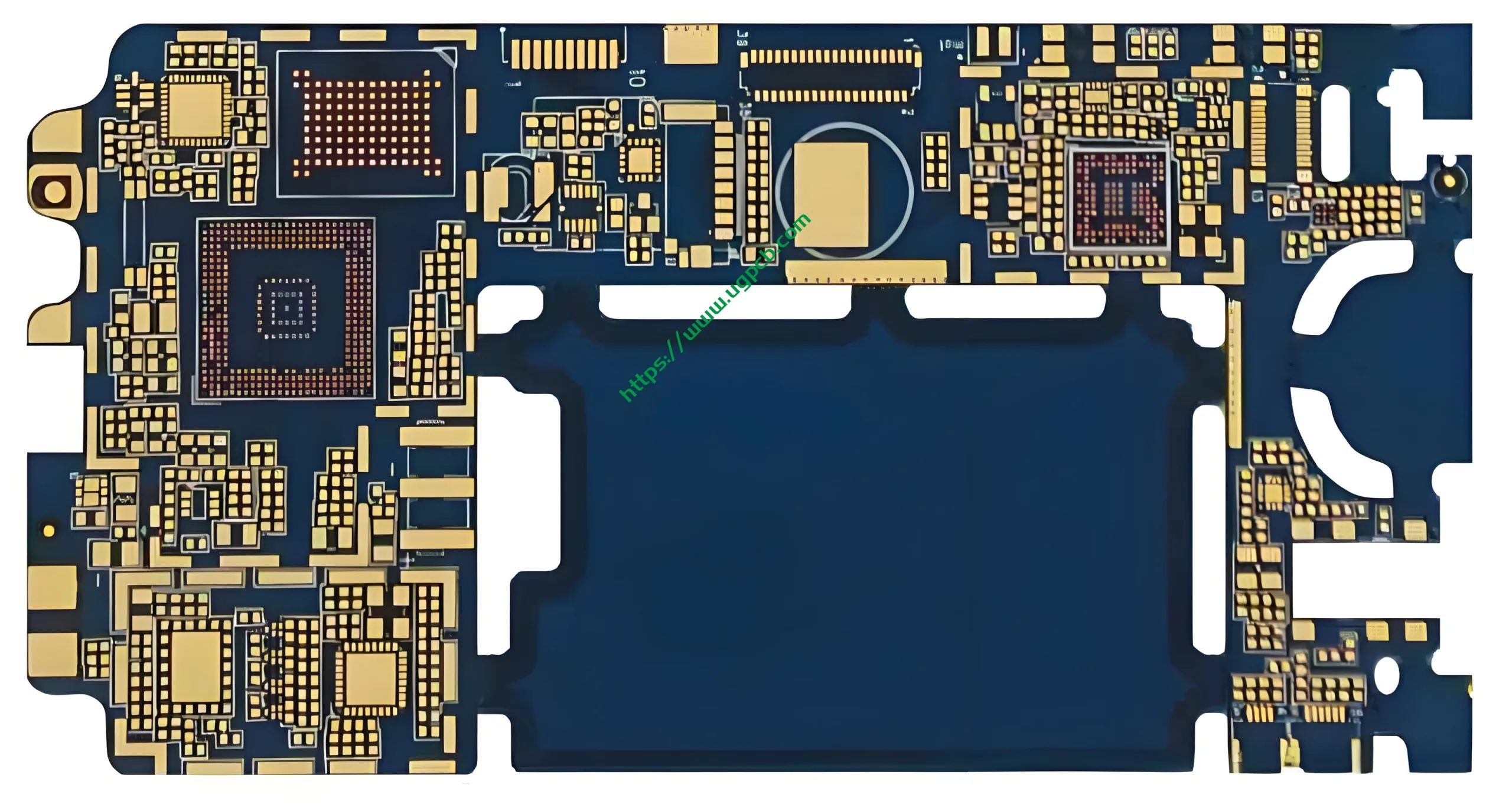
UGPCB’s 2+N+2 Countersink hole HDI 8L PCB with Blind Hole is a high-performance プリント基板 高度な電子アプリケーション用に設計されています. これ プリント基板 integrates high-density interconnect (HDI) technology with countersink holes and blind vias, offering superior reliability for intelligent digital products. With an 8-layer structure, it supports complex designs while maintaining a compact form factor, making it ideal for space-constrained devices. Key parameters include a 1.0mm finished thickness, FR-4材, and immersion gold surface treatment, ensuring durability and efficient signal transmission.
Definition of the Product
This PCB is defined as an 8-layer HDI board featuring a 2+N+2 build-up structure, which refers to two sequential lamination cycles with a core layer (N). It incorporates countersink holes—conical recesses for screw heads—and blind vias that connect outer layers to inner layers without penetrating the entire board. This design enhances routing density and reduces size, catering to modern プリント基板設計 trends for high-speed applications.
Design Key Points
When designing this PCB, critical factors include minimizing trace and space to 3mil/3mil for high-density routing, and adhering to hole size specifications: mechanical holes at 0.2mm and laser-drilled blind holes at 0.1mm. The copper thickness (inner 1OZ, outer 0.5OZ) must balance current carrying capacity and signal integrity. Designers should prioritize thermal management and impedance control, especially for PCBAアセンブリ プロセス, to avoid issues like signal loss. Using HDI PCB design software is recommended to optimize layer stacking and via placement.
作業原則
The PCB operates by facilitating electrical connections between components through its layered structure. Blind holes allow interconnections between specific layers, reducing signal path length and improving speed, while countersink holes provide mechanical stability for mounting components. The HDI technology enables shorter pathways, enhancing performance in high-frequency applications, such as those found in プリント基板 for smart devices.
Applications and Uses

This PCB is widely used in intelligent digital products, including smartphones, 錠剤, ウェアラブルデバイス, and IoT equipment. Its high-density design supports advanced functionalities like 5G connectivity and AI processing, making it a top choice for PCB manufacturers focused on innovation. Applications extend to automotive electronics and medical devices where reliability is critical.
分類
Based on structure, this product falls under the HDI PCB category, specifically a 2+N+2 type with blind and buried vias. It can be classified by layer count (8L), 材料 (FR-4), そして表面仕上げ (浸漬ゴールド + OSP), aligning with industry standards for high-end PCBA solutions.
使用材料
The primary material is FR-4, a flame-retardant epoxy laminate known for its excellent electrical insulation and mechanical strength. Copper foils (1OZ inner, 0.5OZ outer) provide conductivity, while the immersion gold surface treatment offers corrosion resistance and solderability, crucial for PCBA assembly. This material selection ensures the PCB meets RoHS compliance for environmental safety.
性能特性
Performance highlights include high thermal stability, 信号損失が少ない, and impedance control. With a minimum trace width of 3mil, it supports high-speed data transmission. The blind hole technology reduces parasitic capacitance, 信号の整合性の向上. These features make it reliable for demanding PCB applications, such as in high-frequency digital products.
構造の詳細
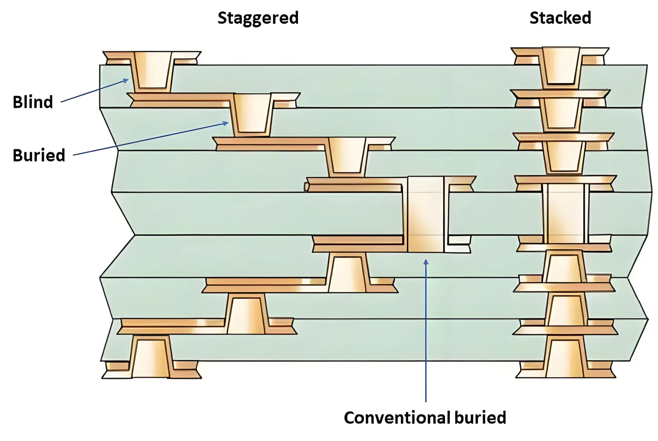
The structure consists of 8 layers with a symmetric build-up: two outer layers connected via blind vias to inner layers, surrounding a core. Countersink holes are machined on the surface for secure component mounting. This layout maximizes space efficiency and supports complex PCBA designs, such as those with BGA components.
主な特長
Key features include miniaturization capabilities, enhanced reliability due to robust via structures, and compatibility with lead-free soldering. The blue or white solder mask aids in inspection, while the 1.0mm thickness ensures durability. These attributes make it a preferred choice for PCB procurement in cutting-edge electronics.
製造工程
The manufacturing process comprises multiple stages: inner-layer imaging, ラミネーション, laser drilling of blind vias, mechanical drilling of counterbore holes, メッキ, and surface finishing. Quality assurance involves electrical testing and automated optical inspection (あおい) to ensure compliance with specifications. This workflow emphasizes precision in HDI PCB production, ensuring high manufacturing yield for subsequent PCBA integration.
使用シナリオ
Common usage scenarios include consumer electronics like smart home devices, industrial automation systems, and communication hardware. It is ideal for applications requiring compact, 高速PCB, such as in PCBA for embedded systems or automotive control units. This versatility supports innovation in PCB-driven technologies.


