
Widespread Usage
The 4-layer HDI PCB is widely used in:
- Telecom module
- Wireless module
- LED display module
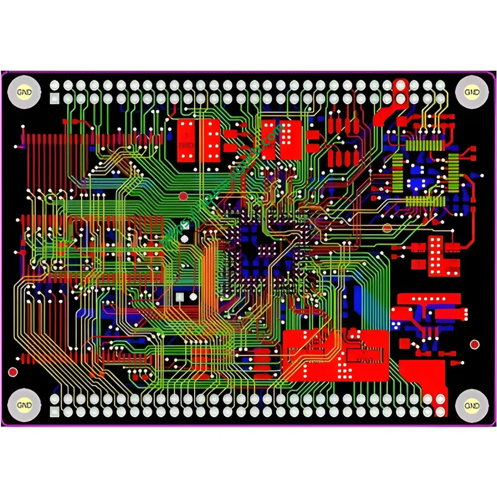
HDI PCB (1+n+1) Layout Design Structure
Basic Description
The HDI PCB (1+n+1) is the simplest HDI PCB layout design structure, suitable for BGAs with fewer I/Os.
特徴
- Fine lines
- Micro vias
- Registration technology capable of 0.4mm ball pitch for excellent mounting stability and reliability
- May contain copper-filled vias
Material and Finish
It is qualified material and finish for lead-free process.


