
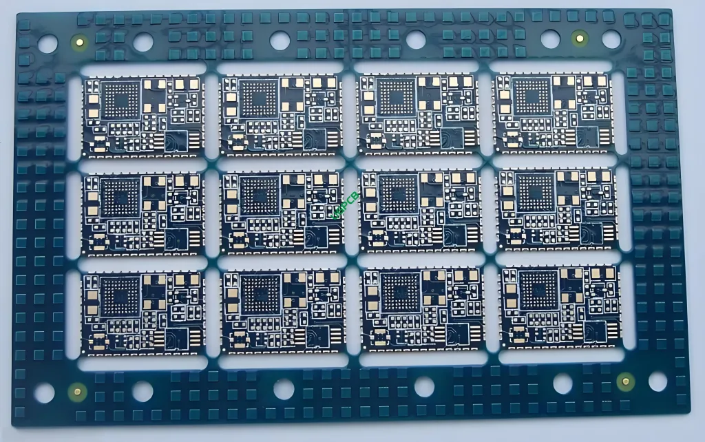
Overview of 4layers Multilayer Bluetooth PCB
The 4-layer multilayer Bluetooth プリント基板 is a specialized product designed to meet the stringent requirements of Bluetooth applications. This type of PCB offers high signal integrity, 熱安定性, と信頼性, making it an ideal choice for various Bluetooth-enabled devices.

意味
A 4-layer multilayer Bluetooth PCB is a プリント基板 specifically designed to support the functions of a Bluetooth module. It consists of multiple layers of conductive and insulating 材料, providing complex electrical pathways and connections essential for the operation of the Bluetooth device. 用語 “4-層” refers to the number of conductive layers, その間 “多層” indicates that it has more than two layers of conductive material.
設計要件
When designing a 4-layer multilayer Bluetooth PCB, いくつかの重要な要件を満たす必要があります:
- 材料品質: 高品質のFR4材料は、耐久性と熱安定性に不可欠です.
- レイヤー構成: 2層の設計が標準です, allowing for efficient routing of signals and power.
- 銅の厚さ: 1オンスの銅の厚さは、適切な導電率を保証します.
- 表面処理: 浸漬金表面処理により、接続性と耐食性が向上します.
- トレース/スペースの寸法: 4milの最小トレースとスペースの寸法 (0.1mm) 正確な回路パターンに必要です.
- 特別な機能: Half-hole PCB design is often incorporated for specific component placement and soldering requirements.
作業原則
The 4-layer multilayer Bluetooth PCB operates based on the principles of electrical conductivity and signal integrity. 導電性層は、電気信号の経路を形成します, 一方、絶縁層は、これらの信号間の不要な相互作用を防ぎます. The half-hole design allows for better signal routing and reduces crosstalk. 浸漬金表面処理は優れた接続性を提供し、環境要因から保護します.
アプリケーション
This type of PCB is primarily used in Bluetooth-enabled devices, which are crucial コンポーネント in various electronic systems such as wireless communication devices, オーディオ機器, and IoT (モノのインターネット) デバイス. これらには含まれます:
- Bluetooth speakers and headphones
- Wireless keyboards and mice
- スマートホームデバイス
- Fitness trackers and wearables
- 産業自動化システム
分類
4-layer multilayer Bluetooth PCBs can be classified based on their specific features and intended use, のような:
- Signal Integrity Boards: For maintaining high signal quality in Bluetooth communications.
- 熱管理板: To efficiently dissipate heat generated by Bluetooth components.
- コントロールボード: For managing and controlling various functions in Bluetooth-enabled systems.
材料
The primary materials used in the construction of a 4-layer multilayer Bluetooth PCB include:
- 基本材料: FR4, 優れた誘電特性と機械的強度で知られている火炎耐性繊維グラスファイバー材料材料.
- 導電性材料: 銅, 導電性トレースに使用されます.
- 表面処理: イマージョンゴールド, 接続を向上させ、耐食性を提供します.
パフォーマンス
The performance of a 4-layer multilayer Bluetooth PCB is characterized by:
- 高い信号の完全性: Due to the precise trace and space dimensions and half-hole design.
- 熱安定性の向上: The FR4 base material helps dissipate heat more effectively.
- 信頼できる接続: 浸漬金表面処理によって保証されます.
- 耐久性: 堅牢なFR4ベース材料によって強化されました.
- 電気効率: 最適化されたレイヤー構成による信号損失と干渉の最小化.
構造
The structure of a 4-layer multilayer Bluetooth PCB consists of:
- 導電性材料の2層: 絶縁層と交互に.
- 浸漬金表面処理: 強化された接続と保護のため.
- ハーフホールデザイン: 特定のコンポーネントの配置とはんだ付け要件について.
特徴
Key features of the 4-layer multilayer Bluetooth PCB include:
- Advanced Layer Configuration: 4-layer design for superior signal routing.
- 高精度: 4milの最小トレースとスペースの寸法を備えています (0.1mm).
- カスタマイズ可能なカラーオプション: 黒または白で利用可能.
- 標準の厚さ: 仕上がり厚さ1.0mm.
製造工程
The production process for a 4-layer multilayer Bluetooth PCB involves several steps:
- 材料の準備: FR4シートと銅ホイルの選択と準備.
- レイヤースタッキング: 銅と絶縁層を組み合わせます.
- エッチング: 過剰な銅を除去して、目的の回路パターンを形成します.
- メッキ: 浸漬金表面処理の適用.
- ラミネート加工: 熱と圧力の下で層を組み合わせます.
- 掘削: スルーホールコンポーネントとVIAの穴を作成します.
- ソルダーマスクの塗布: はんだブリッジと環境要因から回路を保護します.
- シルクスクリーン印刷: コンポーネントの配置と識別のためのテキストとシンボルを追加します.
- 品質管理: PCBがすべての設計仕様と標準を満たすようにします.
シナリオを使用します
The 4-layer multilayer Bluetooth PCB is ideal for scenarios where:
- 高い信号の完全性が重要です.
- 信頼できる耐久性のある接続が必要です.
- 安定した動作温度を維持するには、効果的な熱管理が必要です.
- パフォーマンスを向上させるには、高度な表面処理が必要です.


