

1.UGPCB 4-Layer High Tg Rigid-Flex PCB 製品の概要: Redefining High-Reliability Interconnectivity
In modern high-end electronic design, traditional rigid プリント基板 (プリント基板) are often limited by space and form factor, while Flexible PCBs (FPCS) may lack mechanical support. リジッドフレックス PCB テクノロジー, an innovative プリント基板の製造 解決, perfectly merges the stability of rigid boards with the bendability of flexible circuits. UGPCB 4-Layer High Tg Rigid-Flex PCB, with its precise lamination structure, superior material selection, and demanding surface finish, stands as the ideal PCB solution for complex 3D spatial layouts and harsh operating environments.

2. Scientific Classification & Core Parameters
-
Scientific Classification: あたり IPC標準 and industry norms, this product is accurately classified as a 4-Layer High Thermal Reliability Rigid-Flex Printed Circuit Board.
-
Core Parameters:
-
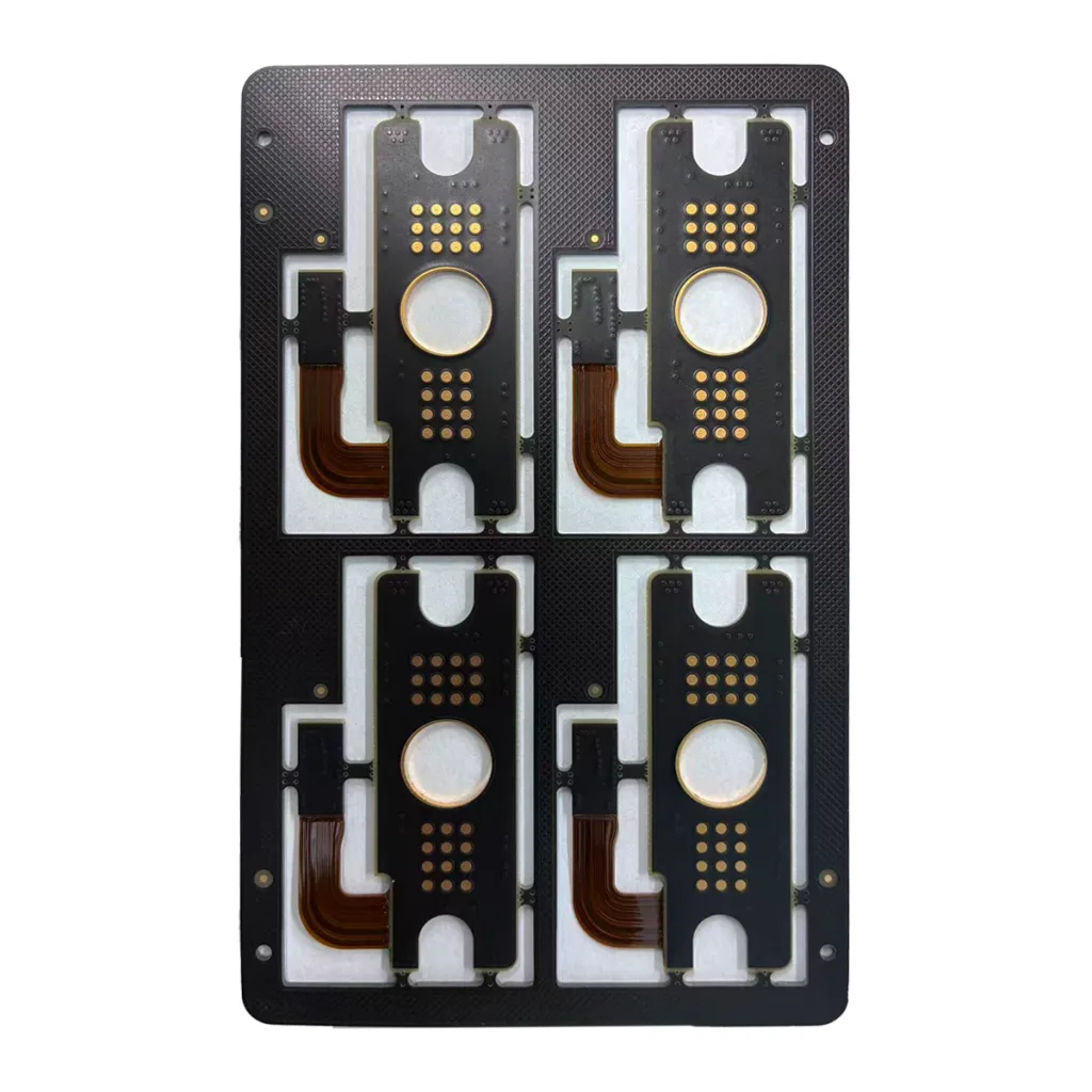
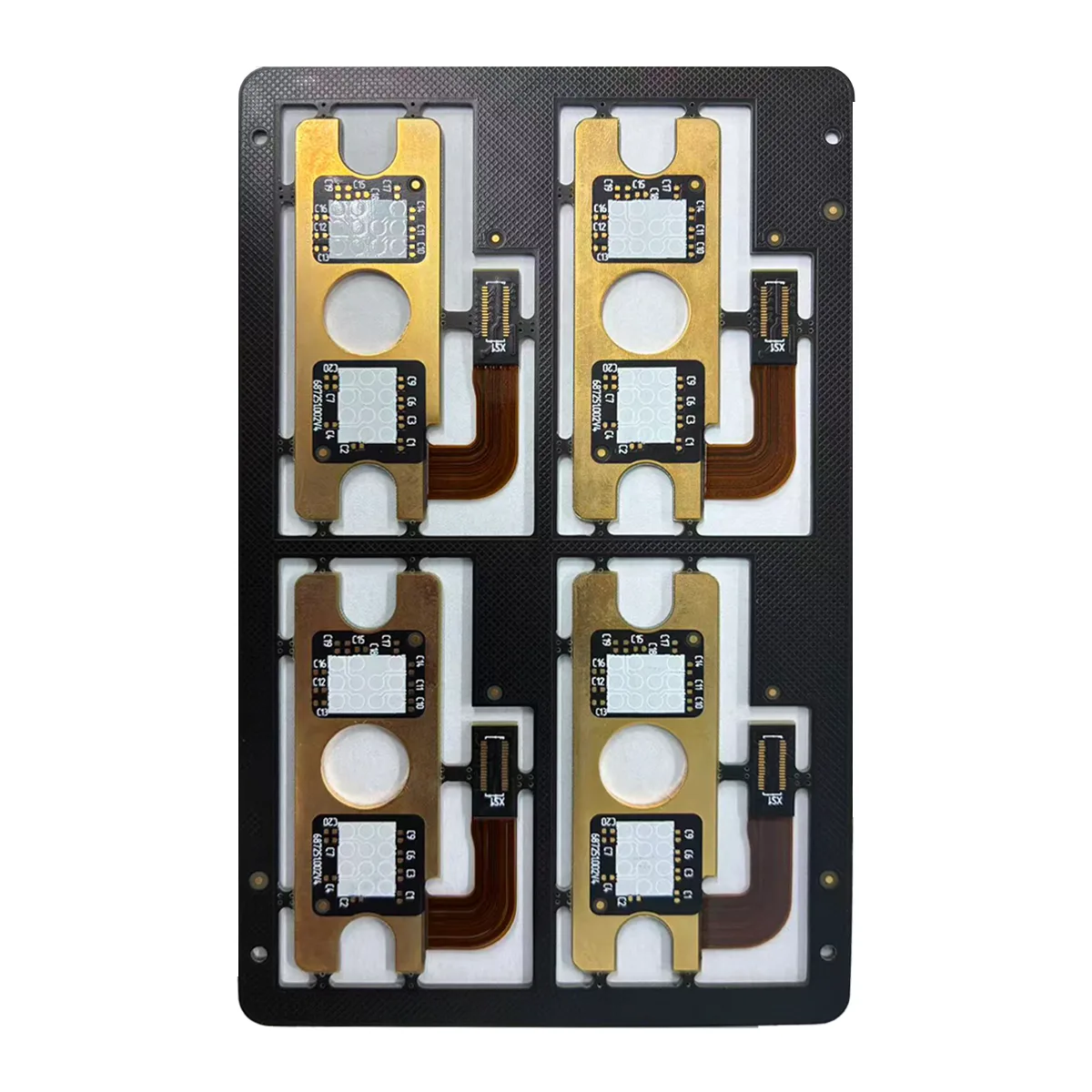
Layer Construction: 4 レイヤー (4L リジッドフレックス PCB)
-
板厚: 1.60mm (in rigid areas, including dielectrics and copper)
-
基本材料: Panasonic RF-777 (35/50µm copper)
-
表面仕上げ: 同意する (エレクトロレスニッケルイマージョンゴールド) 3µ” + Selective Electroplated Hard Gold 30µ”
-
寸法: 126mm * 80mm
-
3. Design Essentials & Structure Analysis
Successful Rigid-Flex PCB design 重要です. This product is designed adhering to these key points:
-
Rigid-to-Flex Transition Zone Design: Bend areas are meticulously simulated, avoiding right and acute angles. Smooth curved traces are implemented to eliminate stress concentration points, a cornerstone of high-reliability PCB design.
-
Stack-up Symmetry: Rigid sections employ a symmetrical lamination stack-up (例えば。, copper-dielectric-core-dielectric-copper) to prevent warping under thermal stress.
-
材料の互換性: The selected Panasonic RF-777 material has matched Coefficients of Thermal Expansion (CTE) in both rigid and flexible zones, ensuring robust bonding at the interfaces.
Structural Feature: The board is constructed by laminating two rigid outer sections with a multilayer structure containing flexible inner layers, enabling electrical interconnection in three-dimensional space.
Image Suggestion 2: A detailed cross-sectional diagram of the board’s layer stack-up, clearly labeling rigid areas, flex areas, 材料, と厚さ.
Alt Tag: Cross-section diagram of a 4-Layer Rigid-Flex PCB stack-up, showing the integration of rigid FR-4 and flexible polyimide materials.
4. 材料 & パフォーマンス
-
コア素材: Panasonic RF-777. This is a high-performance laminate specifically optimized for Rigid-Flex PCB fabrication.
-
高いガラス転移温度 (TG): Provides excellent thermal stability, maintaining mechanical and electrical properties during high-temperature soldering (例えば。, lead-free reflow) and in high-temperature operating environments.
-
低dk (誘電率) & Df (損失係数): Ensures signal integrity for 高周波プリント基板 アプリケーション.
-
Superior Dimensional Stability & 耐薬品性: Guarantees long-term reliability.
-
-
表面仕上げ: ENIG 3µ” + Electroplated Hard Gold 30µ”. This combination is a key differentiator.
-
同意する: アパートを提供します, highly solderable surface finish across the entire board, suitable for fine-pitch component assembly.
-
Electroplated Hard Gold: Applied selectively to connector fingers or areas subject to frequent insertion/withdrawal or friction, the 30µ” hard gold layer dramatically increases wear resistance, 耐酸化性, 信頼性に連絡します, extending connector lifecycle.
-
5. Manufacturing Process Flow
UGPCB employs industry-leading PCB production processes to ensure quality:
-
Laser & Mechanical Drilling: High-precision drilling for varying hole size requirements.
-
ホールメタライゼーション & メッキ: Ensures interlayer connectivity.
-
パターニング & エッチング: Forms precise circuit patterns.
-
ラミネート加工 & Pressing: Precisely bonds rigid and flexible layers into a single unit under high heat and pressure—the technical core of rigid-flex circuit board processing.
-
表面仕上げ: Sequential application of ENIG and selective hard gold plating.
-
Contour Routing & テスト: Final outline achieved via CNC and laser routing, に続く あおい (自動光学検査), 電気試験, and flex-cycle reliability testing.
Image Suggestion 3: An image of a modern PCB production line, focusing on a lamination press or AOI inspection station.
Alt Tag: UGPCB’s modern Rigid-Flex PCB production line featuring high-precision lamination and inspection equipment for quality assurance.
6. 重要な利点 & 製品の特徴
-
3D Design Freedom: Solves complex spatial layout challenges, reduces connectors and cabling, and enhances system reliability.
-
Exceptional Mechanical & 電気性能: High-strength flex joints withstand thousands of dynamic bend cycles; shortened signal paths reduce loss.
-
High Reliability Assurance: High Tg material and dual surface finish ensure stable long-term operation in harsh environments (高温, 湿度, vibration).
-
Weight & Size Reduction: Contributes to overall device miniaturization and lightweight design.
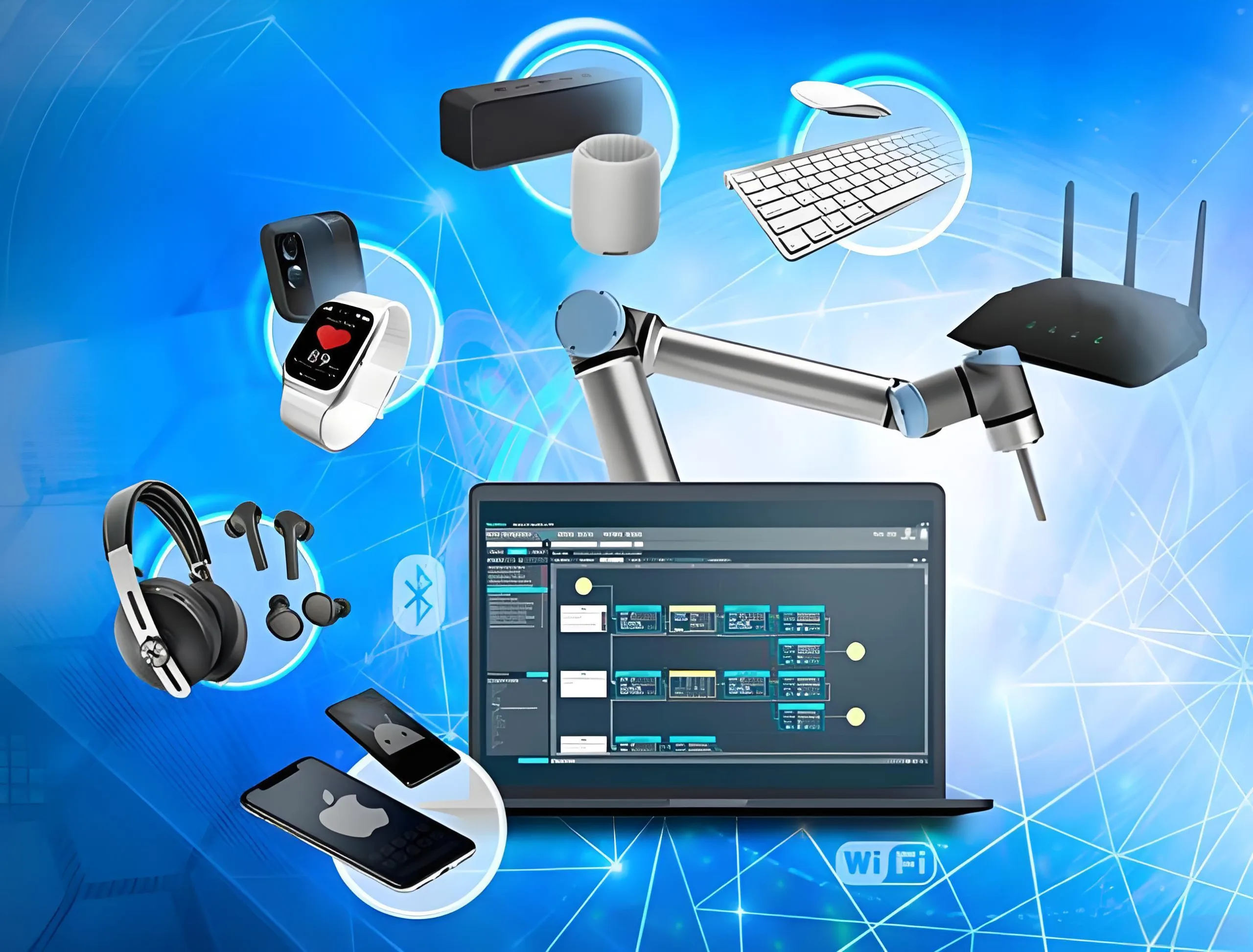
7. 典型的なアプリケーション
これ 4-Layer Rigid-Flex PCB is the preferred PCB component for demanding sectors:
-
産業用 & カーエレクトロニクス: Vibration-resistant connections in control systems, automotive sensors, and Engine Control Units (カバー).
-
医療機器: 内視鏡, portable monitors, hearing aids—devices requiring precise, 信頼性のある, and bendable interconnects.
-
航空宇宙 & 防衛: Avionics and military electronics where weight, 空間, そして信頼性が最も重要です.
-
High-End Consumer Electronics: Camera module connections in smartphones, hinge connections in wearables, advanced digital cameras.

8. UGPCBを選択する理由?
As a professional PCBメーカー, UGPCB を専門とする リジッドフレックス PCB テクノロジー, offering full-spectrum capabilities from PCB design support and precision PCB製造 to rigorous PCB testing. We commit to:
-
Expert Engineering Support: Free PCB design for manufacturing consultation for your project.
-
Consistent, Reliable Quality: Every board undergoes stringent reliability testing.
-
競争力のある価格設定 & Lead Times: Optimized supply chain and production management deliver high-value PCB solutions.
Contact UGPCB today for a free prototype evaluation and quote. Let our professional プリント基板の製造 services power your innovative product to market success.