

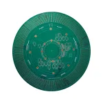
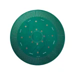
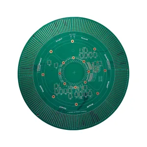
UGPCB の ATE プローブ カード PCB の紹介
UGPCB の 50 層 ATE (自動試験装置) プローブカード プリント基板 高周波半導体テスト用に設計された精密設計のソリューションです. テスト機器と集積回路間の正確な信号伝送を可能にします。 (IC), ミッションクリティカルな環境で信頼性の高いパフォーマンスを確保.
主要な技術仕様
-
レイヤー数: 50 レイヤー
-
厚さ: 198 ミル
-
材料: FR4 HTg (高温ガラスエポキシ)
-
最小穴サイズ: 5 ミル
-
BGA の間隔: 0.35mm
- 銅の厚さ:2/2オンス
-
アスペクト比: 40:1
-
ドリルから銅までの距離: 3 ミル
-
POFV (フィルドビア上にメッキ): はい
-
表面仕上げ: ENEG (無電解ニッケル 無電解金)
デザインと構造の革新
重要な設計機能
-
高密度相互接続: 50層アーキテクチャは、0.35mmピッチのBGAコンポーネントの超微細配線をサポートします。, 最新のICテストに不可欠.
-
先端材料: FR4 HTg により熱安定性が保証されます (ガラス転移温度≧180℃), 高出力試験サイクル中の変形を防止.
-
精密穴あけ: あ 40:1 アスペクト比と 5 ミルマイクロビアにより、密な間隔のレイアウトで信頼性の高い信号パスが実現.
-
POFV テクノロジー: 充填およびメッキされたビアにより機械的強度と熱放散が向上します, 長期間のテスト作業に不可欠.
構造上の利点
-
ドリルから銅線までの超短距離: 3 ミル間隔により信号損失とクロストークを最小限に抑えます.
-
ENEG 表面仕上げ: 優れた耐酸化性と安定した接触面をプローブ針に提供します。.
パフォーマンスと機能アプリケーション
運営原則
PCB は、テストプローブと IC 間の電気信号を最小限の遅延で配線します。. FR4 HTg 基板は熱ストレス下でも誘電体の一貫性を維持します, 一方、POFV は高振動環境でも中断のない接続を保証します。.
キーパフォーマンスメトリック
-
耐熱性: 180℃までの温度でも安定した性能.
-
信号の完全性: 制御されたインピーダンス (±8%) 低挿入損失 (<0.5DB).
-
機械的耐久性: 剥離を防止します。 10,000+ テストサイクル.
主な使用例
-
半導体検査: ロジックチップを検証します, メモリモジュール, およびATEシステムのプロセッサ.
-
航空宇宙エレクトロニクス: 超高信頼性 PCB を必要とする航空電子工学試験装置で使用.
-
5G・IoTデバイスの製造: 高周波 RF コンポーネントのテストで信号の精度を保証します.
-
車載用ICの検証: ADAS および ECU テストのワークフローに導入.
製造工程と品質保証
製造ワークフロー
-
材料の切断: FR4 HTg ラミネートは必要な寸法に精密にカットされます.
-
レーザー穴あけ加工: 達成 5 ミル穴付き 40:1 CO₂ レーザーを使用したアスペクト比.
-
メッキとビア充填: POFV テクノロジーによりビアを銅メッキで強化.
-
レイヤーの配置: 50-層の積層は高圧および高温下で接着されます.
-
表面処理: ENEGコーティングにより耐食性を向上.
-
厳格なテスト: 電気的導通チェックを含む, インピーダンス試験, および熱サイクル検証.
品質基準
-
IPC-6012クラス 3 コンプライアンス: 過酷な産業用途の信頼性を保証.
-
100% 自動光学検査 (あおい): 高密度レイアウトの微小欠陥を検出.
競争上の利点の概要
-
超高密度: 0.35mm BGA間隔で小型ICテストをサポート.
-
熱弾性: FR4 HTg は極端な条件下でも安定性を保証します.
-
業界をリードする精度: 5 ミルマイクロビアと 3 ミルと銅の間隔.
-
幅広い互換性: TeradyneやAdvantestなどの主要なATEプラットフォームと互換性があります.
この PCB は最先端のエンジニアリングを組み合わせています, 厳格な品質管理, 次世代半導体検査の要求を満たす特殊な材料.


