
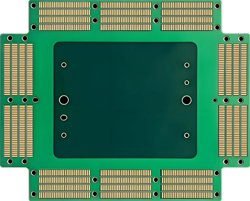
58 層 ATE ロード PCB の概要
58層ATE (自動試験装置) 負荷PCBは高密度です, 多層 プリント基板 要求の厳しいテスト環境での正確な信号伝送と耐久性を実現するように設計されています。. 高度なパラメータを使用して設計, 高周波および高出力アプリケーションで最適なパフォーマンスを保証します。.
主な仕様
-
レイヤー: 58
-
寸法: 17.2″ ×17.8″
-
厚さ: 230 ミル
-
材料: FR4 Tg185
-
最小穴サイズ: 5 ミル
-
BGA の間隔: 0.8 mm
-
アスペクト比: 23.4:1
-
ドリルから銅までの距離: 7 ミル
-
POFV (フィルドビア上にメッキ): はい
-
バックドリリング: いいえ
-
表面仕上げ: ワン+TG+ワン
デザインと構造の特徴
設計上の重要な考慮事項
-
レイヤー数が多い: 58層構造により、高密度相互接続の複雑な配線をサポート (HDI), 信号損失を最小限に抑える.
-
材料の選択: FR4 Tg185 により熱安定性が保証されます (ガラス転移温度185℃まで), 高出力アプリケーションにとって重要.
-
精密穴あけ: あ 5 ミル最小穴サイズと 23.4:1 アスペクト比により信頼性の高いマイクロビア形成が可能, BGAには必須 (0.8 MMピッチ) コンポーネントの統合.
-
信号の完全性: 制御されたインピーダンスと 7 ドリルから銅までのミル間隔によりクロストークと電磁干渉を低減 (エミ).
ユニークな構造上の利点
-
POFV テクノロジー: ビアの充填とメッキによりビアの信頼性を向上, 熱的および機械的性能の向上.
-
ENEG+TG+ENIG 表面仕上げ: 無電解ニッケルと無電解金を配合 (ENEG) そしてイマージョンゴールド (同意する) 優れた耐食性とはんだ付け性を実現.
性能と用途
運営原則
PCB により、正確な電気信号の配線が容易になります。 58 レイヤー, FR4 Tg185 の誘電特性を利用して信号の整合性を維持. POFV は高ストレス環境でも堅牢な接続を保証します, 最適化されたアスペクト比が安定した高周波動作をサポートします。.
キーパフォーマンスメトリック
-
熱抵抗: 185℃までの温度に耐えます.
-
機械的安定性: 高 Tg 材料が熱サイクル下での層間剥離を防止.
-
信号速度: 低損失の誘電体材料により遅延を最小限に抑える.
主な使用例
-
自動試験装置 (食べた): ICやマイクロプロセッサを検証するための半導体テストシステムで使用されます。.
-
航空宇宙と防御: 高い信頼性が求められるレーダーや通信システムに採用.
-
通信: 5Gインフラと高速データ伝送をサポート.
-
カーエレクトロニクス: ADASに統合 (高度なドライバー支援システム) およびEVパワーモジュール.
製造工程と品質保証
製造ワークフロー
-
材料の準備: FR4 Tg185 ラミネートは 17.2 にカットされます。″ ×17.8″ 寸法.
-
レーザー穴あけ加工: 作成します 5 100万個のマイクロビアを搭載 23.4:1 アスペクト比.
-
めっきと充填: POFV テクノロジーにより、フィルドビアに銅メッキが適用されます.
-
レイヤーのスタックアップ: 58 層は高圧下で整列して接着されます.
-
表面仕上げ: 腐食防止のためにENEG+TG+ENIGコーティングが施されています.
-
テスト: 電気的導通, インピーダンス, 熱応力試験が実施されます.
品質管理基準
-
IPC-6012クラス 3: 過酷な環境でも信頼性を確保.
-
インピーダンス制御: ±10%の公差を維持.
利点のまとめ
-
高密度設計: 複雑な回路をコンパクトなスペースでサポート.
-
熱弾性: FR4 Tg185 は極端な条件下でも安定性を保証します.
-
精密工学: 5 ミル穴と 0.8 mm BGA 間隔により、小型コンポーネントの統合が可能になります.
-
多彩な用途: 半導体検査から5Gインフラまで.
この PCB は最先端の設計を組み合わせています, 厳格な製造基準, ミッションクリティカルな産業のニーズを満たす堅牢な素材.


