

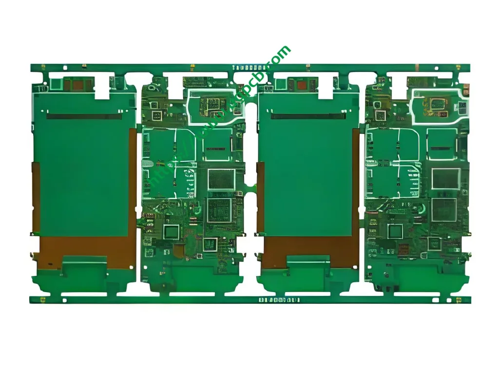
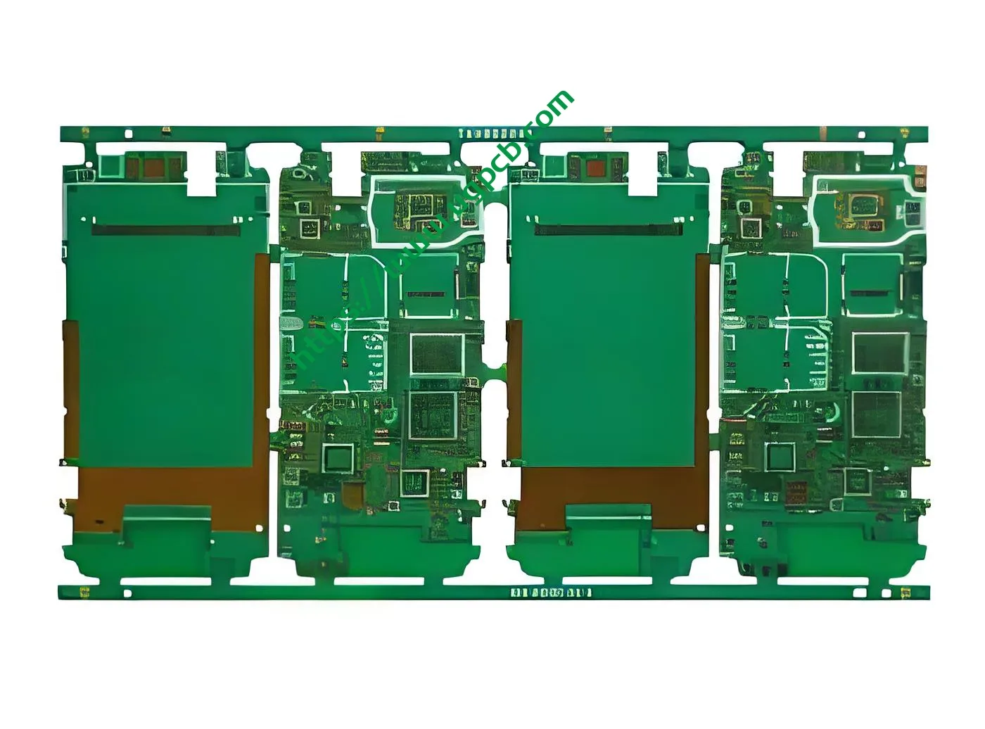
6Layers PCB 1+N+1 HDIの概要
The 6Layers PCB 1+N+1 HDI is a type of high – density interconnect printed circuit board. It plays a vital role in various electronic devices where space – saving and high – quality circuit connections are required.

意味
“6Layers” indicates that this プリント基板 has six layers in total. “1+N+1” represents a specific layer configuration, where “1” stands for a signal layer, “N” can be a combination of signal, 力, または柔軟な方法で地上層, and the last “1” is also a signal layer. “HDI” means High – Density Interconnect, これは、単位面積あたりの電気接続の密度が高いことを意味します.
設計要件
- トレースとスペース: 最小トレースとスペースは3mil/3milに設定されています. この厳格な要件により、正確な回路ルーティングが保証され、隣接する痕跡間の電気干渉のリスクが最小限に抑えられます.
- 穴の寸法: 機械穴は直径0.2mm以下でなければなりません, レーザー穴は少なくとも0.1mmでなければなりません. These dimensions are crucial for proper component mounting and layer – to – layer connections.
作業原則
電気信号は、異なる層の銅の痕跡を介して送信されます. VIAは、さまざまなレイヤーのトレースを接続するために使用されます, コンパクトスペース内で複合回路を実装できるようにする. 電力と地上飛行機は、電力を均等に分配し、電磁干渉を減らすのに役立ちます.
用途
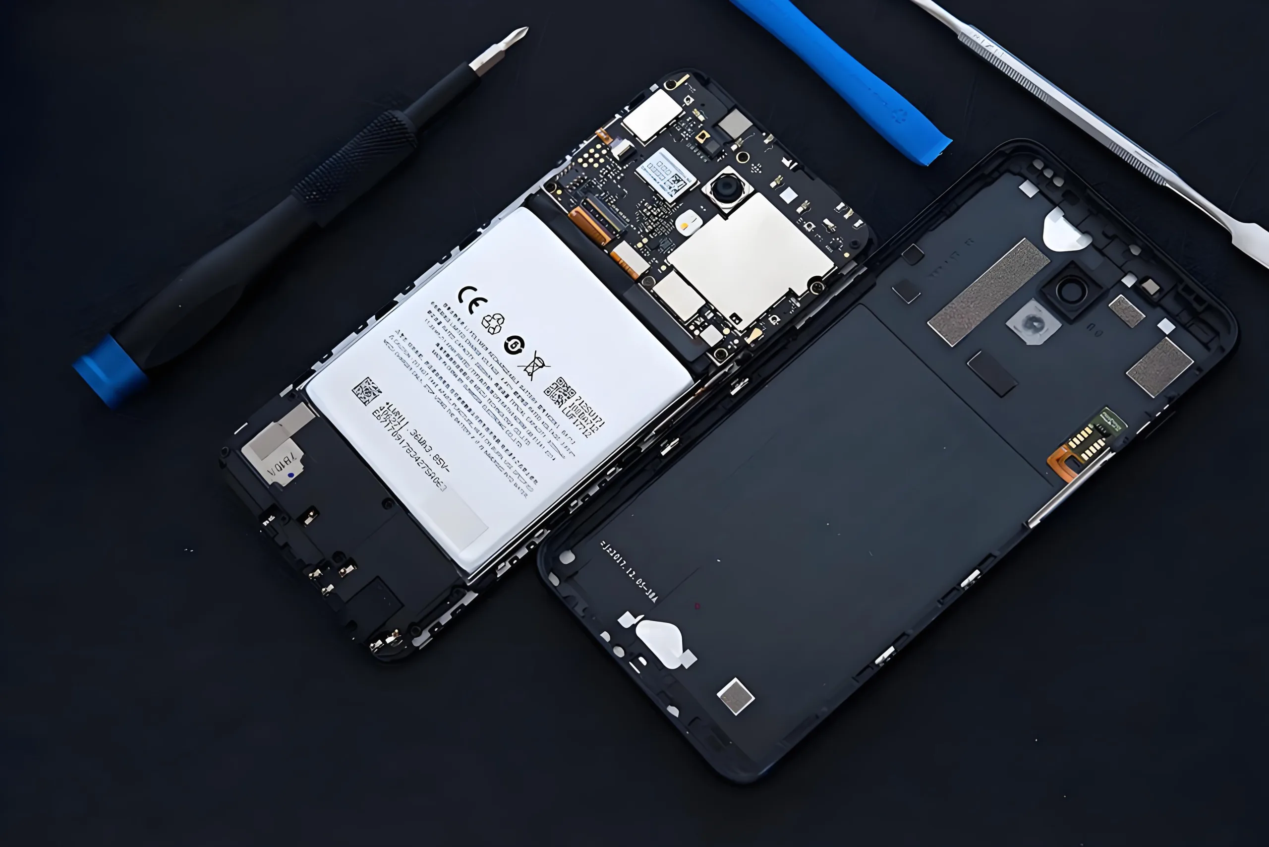
主にモバイルメインボードPCBに使用されます. 携帯電話で, このPCBは、通信などの複数の機能を処理できます, 処理, and sensor integration due to its high – density layout.

分類
It belongs to the multi – layer PCB category within the HDI PCBs. 1+n+1レイヤー構成は、その分類の明確な機能です.
材料
The material is FR – 4. この素材は、優れた機械的強度を提供します, 電気断熱, そして耐熱性, 電子デバイスの安定した動作に不可欠です.
パフォーマンス
- 電気性能: 内側の銅の厚さは1オンスと外側0.5オンスです, 電気信号を効果的に送信できます. 浸漬金表面処理は、優れた電気伝導率も備えており、成分の良好なはんだき性を促進します.
- 機械的性能: The FR – 4 ベースは、モバイルデバイスでの取り扱いとインストールに耐えるのに十分な機械的安定性を提供します.
構造
合計で6つのレイヤーがあります. 通常、2つの外側の層は、信号または電力/地上接続に使用されます, and the “N” layer in the middle can be customized according to the specific circuit design needs.
特徴
- コンパクトレイアウト: Due to its high – density design, それはより多くのコンポーネントをより小さな領域に収容できるようにします.
- 良い表面仕上げ: 浸漬金処理は耐食性と良いはんだしを提供します.
- 柔軟な構成: 1+n+1層の配置は、さまざまな回路設計要件を満たすように調整できます.
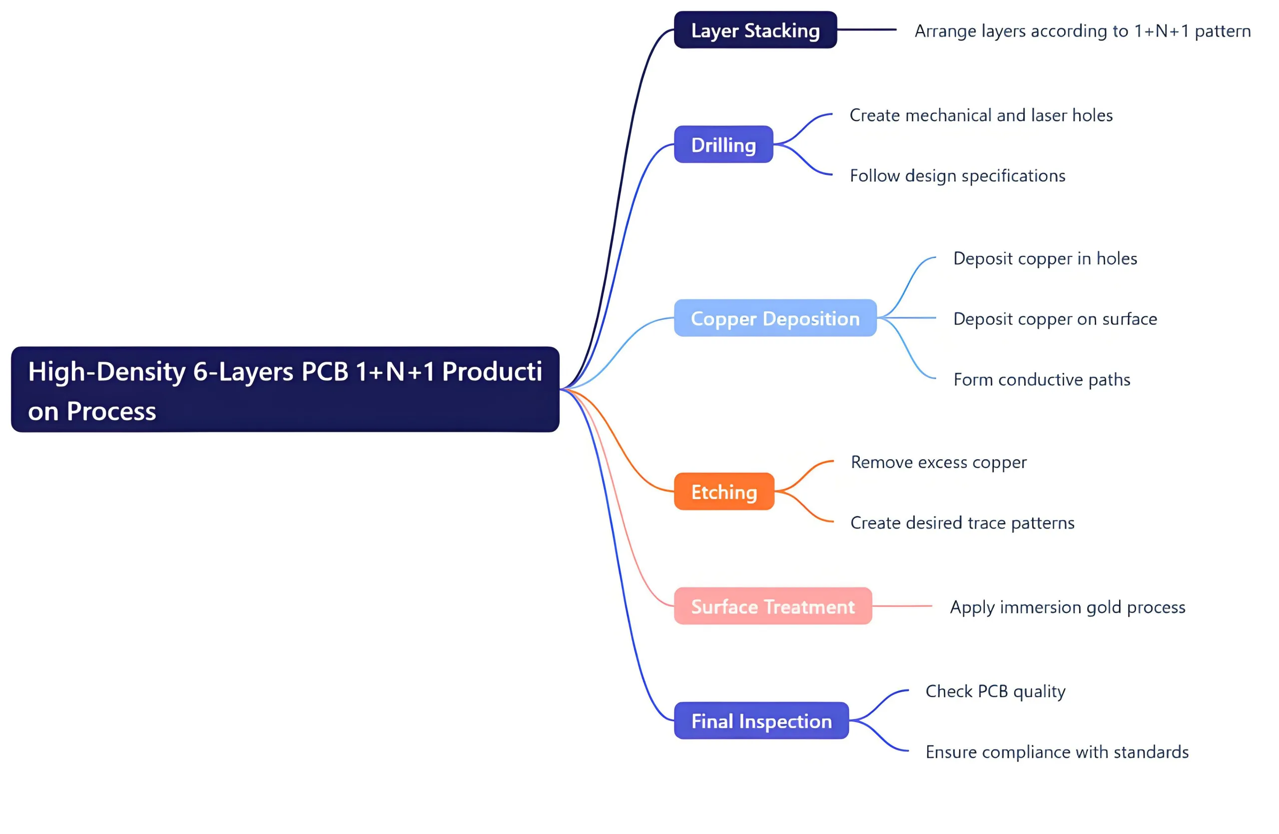
製造工程
- レイヤースタッキング: 1+n+1パターンに従って正確に6つの層を配置します.
- 掘削: 設計仕様に従って、機械式とレーザーホールを作成する.
- 銅の堆積: 穴と表面に銅を堆積させて導電性経路を形成する.
- エッチング: 余分な銅を削除して、目的のトレースパターンを作成します.
- 表面処理: Immersion Goldプロセスを適用します.
- 最終検査: PCBが品質を確認し、すべての標準を満たしていることを確認してください.

使用シナリオ
モバイルメインボードとは別に, it can also be used in other small – form – factor electronic devices such as small portable media players or some compact Bluetooth devices where space is limited but reliable circuit connections are needed.