
構造と構成
The high-frequency hybrid pcb board splint includes a base plate, 折り畳まれ、最初の内側のワイヤレイヤーに配置されます, 最初の外側のワイヤ層, and the top surface of the solder mask ink layer from bottom to top in order from top to bottom. The positioning circuit layer, the second outer wire layer, the bottom surface of the substrate, and the second layer of solder resist ink layer are also part of its structure.
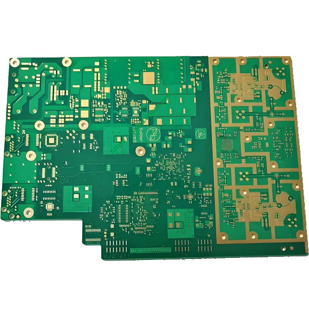
Division of Areas
基板には、高周波エリアと補助領域が含まれます. 補助領域が最終的に固定されます, and the high-frequency area inlay should be located in a fixed position.
Utility Model
ユーティリティモデルは、高周波ハイブリッドスプリントを提供します, 2つの部分に分かれています: 高周波エリアと補助エリア. 機械的なサポートを提供します.
高周波エリアの独立した配置
ユーティリティモデルは、高周波エリアが独立して配置されていることを明らかにしています, そして、高周波領域のみが高周波材料でできています. 高周波信号を満たす条件下で, the use of high-frequency board materials is minimized and the production cost is reduced.
高周波ハイブリッド製品分類
仕様
- レイヤー: 6 レイヤー
- 使用済みボード: ロ4350b + FR4
- 厚さ: 1.6mm
- サイズ: 210mm*280mm
- 表面処理: 金メッキ
- 最小開口: 0.25mm
応用
- 応用: コミュニケーション
特徴
- 特徴: High Frequency Mixed pcb board


