
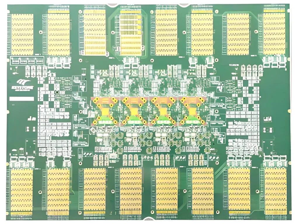
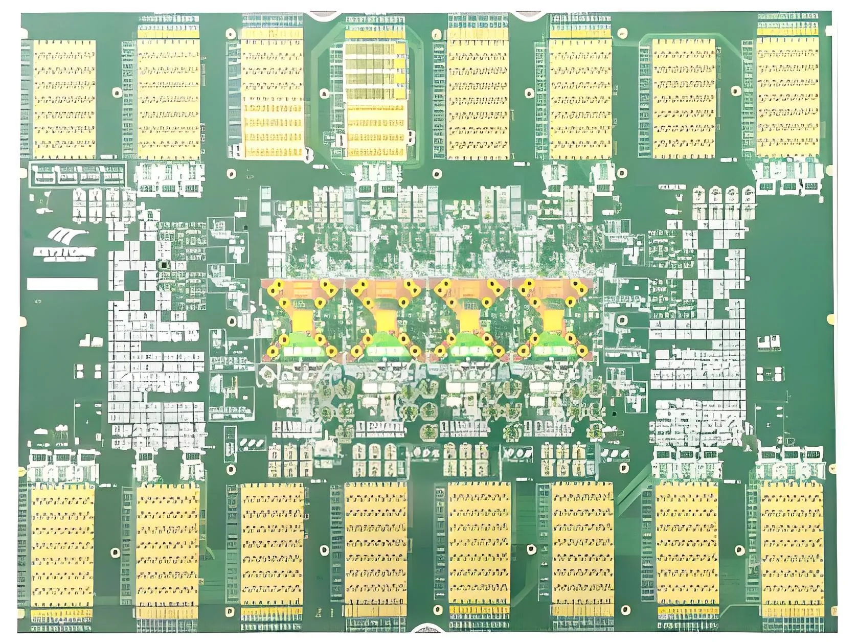
62 層 ATE ロード PCB の概要
62 層 ATE ロード PCB は高性能です, 超高密度 プリント基板 自動試験装置用に設計 (食べた) システム. 複雑な信号ルーティングと高電力負荷を処理するように設計されています, 半導体製造および高度なエレクトロニクス検証における厳しいテスト要件を満たします。.
キーの定義
ATE ロード PCB は、 専用回路基板 集積回路をテストするための実際の動作条件をシミュレートします (IC) そして 電子コンポーネント. 62層構成で複雑な信号経路をサポート, 配電, コンパクトな設計での熱管理.
重要な設計パラメータ
-
レイヤー数: 62 マルチドメイン信号分離と電源プレーン最適化のためのレイヤー.
-
寸法: 16.9″ ×22.9″ (マルチデバイス統合のためのラージフォーマット).
-
厚さ: 250 ミル (剛性と放熱性のバランスをとる).
-
材料: FR4 HTg (180℃までの安定性を実現する高温ガラスエポキシ).
-
最小穴サイズ: 8 ミル (高密度相互接続をサポート).
-
BGA ピッチ: 0.65mm (ファインピッチ部品実装が可能).
-
アスペクト比: 32:1 (マイクロビアの信頼性の高いメッキを保証します).
-
ドリルから銅まで: 7 ミル (短絡を防止します).
-
POFV & バックドリリング: 高周波アプリケーションでの信号歪みを除去します。.
-
表面仕上げ: ENEG (無電解ニッケル 無電解金による耐食性).
コア機能
The プリント基板 ATE システムとテスト対象デバイスの間でテスト信号をルーティングします。 (DUT), 正確な電圧/電流測定を保証する. バックドリルにより未使用のビアスタブを削除し、信号の反射を最小限に抑えます。, POFVしながら (充填ビア上にメッキ) 熱伝導率と構造的完全性を向上させます.
主要なアプリケーション
-
半導体検査: IC を検証します, CPU, およびメモリモジュール.
-
航空宇宙 & 防衛: ミッションクリティカルな航空電子工学およびレーダー システム.
-
通信インフラ: 高速データ伝送装置.
-
医療機器: 高精度の診断および画像ツール.
材料上の利点
FR4 HTg が提供するもの:
-
熱弾性: 周期的な熱ストレス下でも安定した性能.
-
低誘電損失: 高周波信号の完全性にとって重要.
-
機械的強度: 多層ラミネート時の反りに強い.
構造的特徴
-
ハイブリッドスタックアップ: 高速性を兼ね備える, 力, とグランド層.
-
Microviaテクノロジー: レーザーで穴開けされたマイクロビア (8 ミル) 高密度の層間接続を可能にする.
-
制御されたインピーダンストレース: 0.65mm BGA レイアウトでのクロストークを最小限に抑える.
パフォーマンスのハイライト
-
信号の完全性: <3% での挿入損失 10 GHz.
-
パワーハンドリング: 電源プレーンあたり 20A をサポート.
-
熱管理: 1.2 POFV による W/mK 熱伝導率.
製造ワークフロー
-
材料の準備: FR4 HTg コアとプリプレグ シートを切断します。.
-
レーザー穴あけ加工: ±1 ミルの公差で 8 ミルのマイクロビアを作成.
-
メッキ & POFV: ビアを電気メッキし、導電性エポキシで充填する.
-
バックドリリング: 深さ制御されたドリルを使用してスタブを介して余分な部分を除去します.
-
ラミネート加工: プレス 62 高温/高圧下の層.
-
表面仕上げ: はんだ付け性と耐酸化性を高めるためにENEGを適用.
-
テスト: インピーダンスを検証する, 連続, および熱サイクル.
理想的な使用例
-
高周波ATEシステム: 5G RF コンポーネントとミリ波デバイスをテストします.
-
マルチサイトテスト: の並行検証 16+ 単一ボード上の DUT.
-
過酷な環境: 石油/ガス探査センサーと自動車 ECU テスト.


