
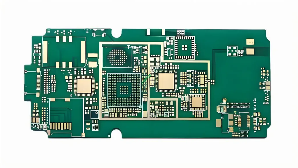
Introduction to the 6L 2+N+2 HDI Product
The 6L 2+N+2 HDI product is a 高密度相互接続 (HDI) プリント基板 (プリント基板) designed for advanced communication applications. This guide provides a comprehensive overview of its specifications, 設計要件, 働く原則, 使用シナリオ, and manufacturing process.

定義と設計の要件
モデル: 6L2+N+2 HDI
This model refers to a six-layer プリント基板 2 つの内部電源層を備えた (2+N), 2つの外部信号層, and two additional high-density interconnect layers. それから’ 内部信号層の数を表します, これは特定のアプリケーションのニーズに応じて変わる可能性があります.
材料: FR-4 アイテック IT180A
The 基本材料 使用したのはFR-4 ITEQ IT180A, 優れた熱安定性で知られています, 機械的強度, そして炎の抵抗.
層構成: 6L2+N+2 HDI
This indicates a six-layer structure with specific layer arrangements for optimized signal integrity and power distribution.
仕上がり厚さ: 1.0mm
完成したPCBの総厚さはです 1.0 ミリメートル, さまざまなアプリケーションの柔軟性を維持しながら耐久性を確保します.
銅の厚さ: 内側の1オンス, 外側0.5oz
内層の銅の痕跡は厚さを持っています 1 オンス (オンス), 一方、外側の層はより薄いです 0.5 oz銅, 導電率と空間効率のバランス.
働く原則と目的
表面処理: イマージョンゴールド + OSP
はんだき性を高め、酸化から保護します, the PCB undergoes immersion gold plating combined with Organic Solderability Preservatives (OSP).
最小トレース/スペース: 2.5ミル/2.5ミル
PCBは、最小トレース幅と間隔で細かいピッチコンポーネントをサポートします 2.5 ミル (1000分の1インチ), パフォーマンスを損なうことなくコンパクトなデザインを促進します.
最小穴の直径: 機械穴0.2mm, レーザーホール0.1mm
0.1mmで0.2mmおよびさらに細かいレーザードリル穴までの機械的掘削を介して小さなコンポーネントを収容します, 高密度統合を有効にします.
応用: 通信製品PCB
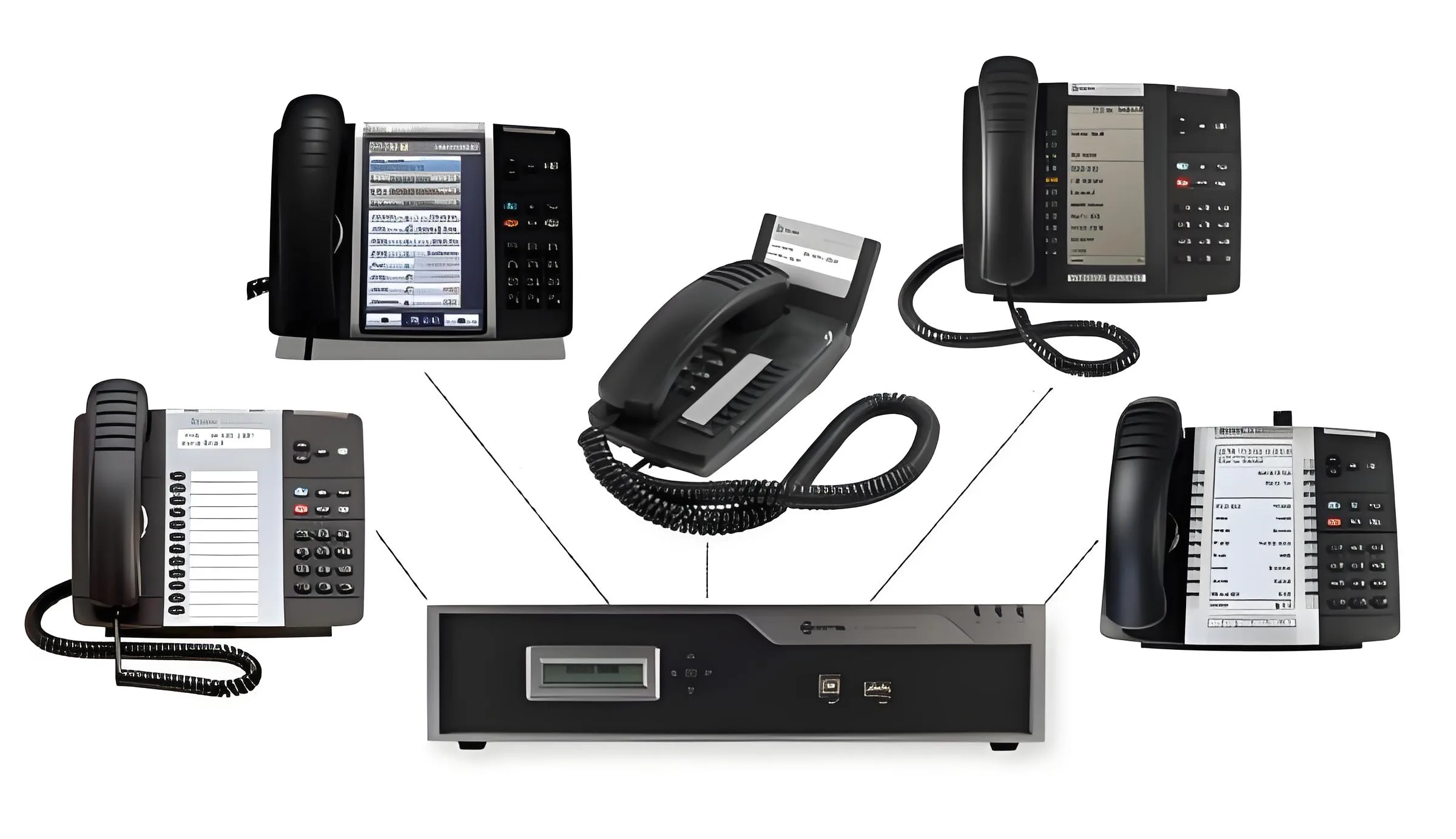 Primarily tailored for communication devices, このPCBは、信頼できる信号伝送と最小限の干渉を保証します, crucial for maintaining clear and consistent data flow in telecommunications systems.
分類と資料
分類: 高密度相互接続 (HDI) プリント基板
HDI PCBとして, 複雑なルーティングとコンポーネントの配置を必要とする複雑な電子デバイス専用に設計されたボードのカテゴリに属します.
材料: FR-4 アイテック IT180A
FR-4は広く使用されている複合材料です。 プリント基板の製造 電気的特性のバランスにより, 熱抵抗, および費用対効果. 具体的なグレード, アイテック IT180A, 一貫した品質とパフォーマンスをさらに保証します.
パフォーマンスと構造
パフォーマンス: 優れた信号の完全性
慎重に設計されたレイヤースタックと高品質の材料の使用により, the 6L 2+N+2 HDI PCB guarantees exceptional signal integrity, クロストークと電磁干渉の削減 (エミ).
構造: 多層配置
構造は、電力面を信号層から分離するように戦略的に配置された複数の層で構成されています, ノイズの最小化と全体的な回路パフォーマンスの向上. HDIテクノロジーを含めると、コンパクトなフォームファクター内でより複雑な設計が可能になります.
機能と生産プロセス
特殊加工: Half Hole Package Edge
A unique feature involves the use of half hole packaging along the edge, which optimizes space utilization and improves connectivity options for edge-mounted components or connectors.
製造工程: 精密製造
 製造は材料の選択から始まり、精密な掘削を続けます, メッキ, およびラミネートプロセス. 各ステップは、厳しい許容範囲と高水準の遵守を確保するために細心の注意を払って制御されています.
典型的なユースケースとシナリオ
典型的なユースケース: 通信機器
Commonly employed in telecommunication infrastructure such as routers, スイッチ, and base stations, where high-speed data transfer and signal reliability are paramount.
使用シナリオ: 高周波アプリケーション
Suitable for applications involving high-frequency signals, including wireless communication modules and RF components, where minimizing signal loss and maximizing bandwidth efficiency are critical.
結論は, the 6L 2+N+2 HDI PCB stands out as a sophisticated solution for demanding communication product requirements, 比類のない密度を提供します, パフォーマンス, and reliability tailored to modern telecommunications needs.


