
Any Layer HDI PCB: The Most Complex Design Structure
概要
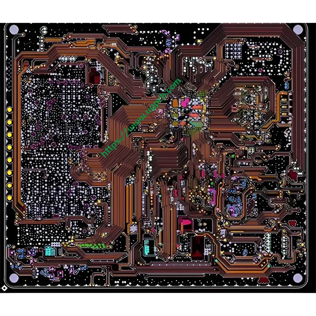
Any Layer HDI PCB is the most complex HDI PCB design structure, offering unparalleled connectivity and performance.
High-Density Interconnect Layers
All Layers as HDI
In this structure, all layers are high-density interconnect layers, allowing for free interconnection of conductors on any layer of the PCB.
Copper-Filled Stacked Microvia Structure
The copper-filled stacked microvia structure facilitates this interconnectivity, providing a reliable and efficient means of connecting various layers.
アプリケーション
Highly Complex Devices
This structure is ideal for highly complex, high pin-count devices such as CPU and GPU chips used in handheld and mobile devices.
Excellent Electrical Characteristics
The design yields excellent electrical characteristics, 高性能アプリケーションに適しています.
利点
Reliable Interconnect Solution
The Any Layer HDI PCB structure provides a reliable interconnect solution for complex devices, ensuring stable and efficient performance.
UGPCBアドバンテージ
この構造, featuring UGPCB technology, represents a significant advancement in PCB design and manufacturing.


