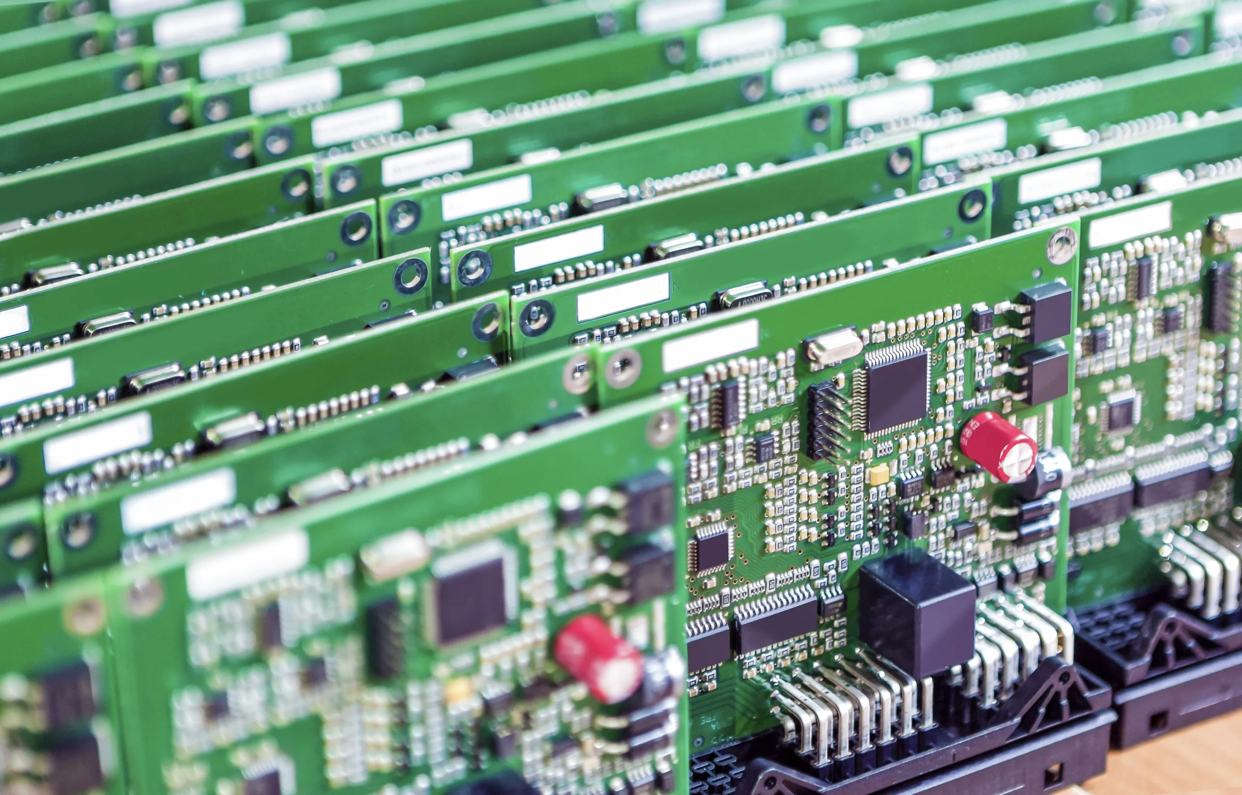
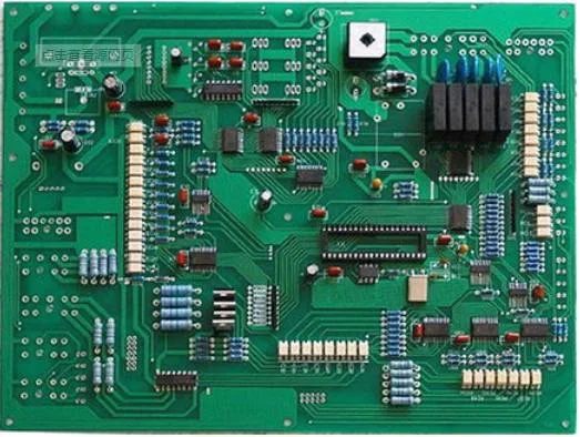
通信機器PCBアセンブリ, 中国の名前は印刷回路基板です, 印刷回路基板とも呼ばれます, 重要な電子コンポーネントです, 電子コンポーネントのサポート, 電子部品の電気接続のためのキャリア. 電子印刷を使用して作られているからです, それはaと呼ばれます “印刷された” 回路基板.
効果
電子機器が印刷されたボードを採用した後, 同様の印刷ボードの一貫性があるため, 手動配線のエラーは回避されます, 電子コンポーネントの自動挿入または配置, 自動はんだ, 電子機器の品質を確保するために自動検出を実現できます. , 労働生産性を向上させます, コストを削減します, メンテナンスを促進します.
開発する
印刷回路基板アセンブリは、単一層から両面に発達しました, マルチレイヤーと柔軟性, そして、それでも独自の開発動向を維持しています. 高精度の方向に継続的に発達しているため, 高密度と高い信頼性, サイズが継続的に減少します, コスト削減とパフォーマンスの改善, 印刷されたボードは、将来の電子機器の開発においてまだ強い活力を維持しています.
印刷されたボード製造技術の将来の開発動向に関する国内および外国の議論の要約は、基本的に同じです, つまり, 高密度に, 高精度, 細かい絞り, 薄いワイヤー, ファインピッチ, 高い信頼性, 多層, 高速トランスミッション, 軽量, 薄さの方向に発達します, また、生産性を向上させる方向に発展しています, コストの削減, 汚染の削減, 多変量と小型バッチの生産に適応します. 印刷回路の技術開発レベルは、一般にライン幅で表されます, 開口部, プリント回路基板のボードの厚さ/開口比.
ソース
印刷された回路基板の作成者はオーストリアのポールアイスラーでした, 誰が最初にラジオでそれを使用しました 1936. で 1943, アメリカ人は主にこの技術を軍事無線に適用しました. で 1948, 米国はこの発明を商業用に公式に認めた. プリントサーキットボードは1950年代半ばから広く使用されています.
PCBの出現前, 電子コンポーネント間の相互接続は、ワイヤの直接接続によって行われました. 今日, ワイヤーは、実験室の実験用途にのみ存在します; プリントサーキットボードは、エレクトロニクス業界で絶対的な制御の位置を確実に占めています.
PCB生産プロセス
メーカーに連絡してください
まず、メーカーに連絡する必要があります, そして、顧客番号を登録します, その後、誰かがあなたのために引用します, 注文します, 生産の進捗状況をフォローアップします.
切断
目的: エンジニアリングデータの要件に従ってMI, 要件を満たす大きなシートを小さな断片に切り、シートを生産する. 顧客の要件を満たす板金の小片.
プロセス: 大きなシート→MI要件に応じて切断→巻き毛シート→ビールの切り身 /エッジ研削→シートの出力
掘削
目的: エンジニアリングデータによると, 必要なサイズを満たすシート材料の対応する位置に、目的の穴の直径を掘削する.
プロセス: Stacking pins→upper board→drilling→lower board→inspect\repair
浸漬銅
目的: 浸漬銅は、化学的方法によって絶縁穴の壁に銅の薄い層を堆積させることです.
プロセス: 粗い粉砕→吊り下げプレート→浸漬銅自動ライン→下のプレート→浸漬 % 希釈H2SO4→肥厚銅
グラフィック転送
目的: グラフィック転送は、制作フィルムの画像をボードに転送することです
プロセス: (青いオイルプロセス): 研削板→最初の側面の印刷→乾燥→2番目の側面の印刷→乾燥→暴露→写真→チェック; (ドライフィルムプロセス): ヘンプボード→プレスフィルム→停止→ペアのビット→露出→休憩→開発→チェック
グラフィックメッキ
目的: パターンの電気めっきは、必要な厚さと、回路パターンの露出した銅の皮膚または穴の壁に必要な厚さの金ニッケルまたは錫層を持つ銅層を電気めたにすることです.
プロセス: 上部プレート→脱脂→水洗浄2回→マイクロエッチング→水洗浄→漬物→銅めっき→水洗浄→漬物→ピクリング→スズめっき→水洗浄→下板
映画を撤回する
目的: NAOHソリューションを使用して、アンチメッキコーティング層を除去して、非ライン銅層を露出させます.
プロセス: ウォーターフィルム: 挿入フレーム→アルカリに浸す→すすぎ→スクラブ→パスマシン; ドライフィルム: ボード→パスマシンを入れます
エッチング
目的: エッチングは化学反応方法を使用して、非回路部品の銅層を腐食させることです.
グリーンオイル
目的: グリーンオイルは、緑色のオイルフィルムのパターンをボードに移し、回路を保護し、部品を溶接するときに回路のスズを防ぐことです
プロセス: 研削板→印刷光感受性グリーンオイル→カーリングボード→露出→発展途上の影; 研削板→最初の側の印刷→ベーキングボード→セカンドサイドの印刷→ベーキングボード
キャラクター
目的: キャラクターは、見やすいマークとして提供されます
プロセス: グリーンオイルを終えた後→冷却と立って→スクリーンの調整→印刷文字→キュリウムの仕上げ
金色の指
目的: Plating a layer of nickel\gold with the required thickness on the plug finger to make it more hard and wear-resistant
プロセス: ボード→脱脂→水洗浄2回→マイクロエッチング→水洗浄2回→漬物→銅メッキ→水洗浄→ニッケルメッキ→水洗浄→金めっき
錫プレート (並列プロセス)
目的: haslは、はんだレジスト油で覆われていない露出した銅表面に鉛とスズの層を噴霧し、腐食や酸化から銅の表面を保護する, 良いはんだパフォーマンスを確保するために.
プロセス: マイクロエッチング→空気乾燥→予熱→ロジンコーティング→はんだコーティング→熱気レベリング→空冷→洗浄および空気乾燥
形にする
目的: 顧客が必要とする形状を形成するための金型スタンピングまたはCNC工作機械を通して. オーガニックゴング, ビールボード, ハンドゴング, とハンドカット
説明: データゴングマシンボードとビールボードの精度が高くなっています, その後、ハンドゴンが続きます, そして、ハンドカットボードはいくつかの単純な形を作ることができます.
テスト
目的: を通して 100% 電子テスト, 視覚的に検出するのが難しいオープンサーキットや短絡などの機能に影響する欠陥を検出する.
プロセス: アッパー金型→ボード配置→テスト→資格→FQC目視検査→資格→修理→リターンテスト→OK→REJ→スクラップ
最終検査
目的: を通して 100% ボードの外観欠陥の目視検査, マイナーな欠陥を修復します, 問題があり、欠陥のあるボードの流出を避けるため.
特定のワークフロー: 着信材料→データのチェック→目視検査→資格→FQAスポットチェック→資格→梱包→資格→処理→OKチェック
業界の傾向
PCB業界は急速に発展しています
改革と開放以来, 中国は、労働資源の観点から優先的な政策により、欧州およびアメリカの製造業の大規模な移転を引き付けました, 市場, 投資. 関連産業の開発. 中国CPCA統計によると, で 2006 私の国のPCBの実際の出力に達しました 130 百万平方メートル, の出力値があります 12.1 10億米ドル, 会計 24.90% グローバルPCB出力値の, 日本を超えて世界のナンバーワンになります. から 2000 に 2006, 中国のPCB市場の平均年間成長率に達しました 20%, 世界平均をはるかに超えています. 世界的な金融危機 2008 PCB業界に大きな影響を与えました, しかし、それは中国のPCB産業に壊滅的な打撃を与えませんでした. 国家経済政策によって刺激されました, 中国のPCB業界は完全に回復しました 2010. で 2010, 中国のPCB出力値に達しました 19.971 10億米ドル . プリマークは、中国が複合年間成長率を維持すると予測しています 8.10% 間 2010 そして 2015, これは、世界の平均成長率よりも高い 5.40%.
地域の分布は不均一です
中国のPCB産業は、主に中国南部と中国東部に分配されています. 2つの合計に到達します 90% 国の, そして、産業凝集効果は明らかです. この現象は、主に中国のエレクトロニクス産業の主要な生産基地がパールリバーデルタとヤンツェ川デルタに集中しているという事実に関連しています。.
PCBダウンストリームアプリケーション分布
中国のPCB業界におけるダウンストリームアプリケーションの分布を以下の図に示します. コンシューマーエレクトロニクスは最も高い割合を占めました, 到達 39%, その後、コンピューターが続きます, 会計 22%, 通信会計 14%, 産業制御/医療機器の会計 14%, 自動車用電子機器の会計 6%, 国防と航空宇宙会計 5%.
後方技術
中国は現在、産業規模の面で世界でナンバーワンですが, PCB業界の全体的な技術レベルの観点から、それはまだ世界の高度なレベルに遅れをとっています. 製品構造の観点から, マルチレイヤーボードは、ほとんどの出力値を占めています, しかし、それらのほとんどはローエンドの製品であり、 8 レイヤー. HDI, 柔軟なボード, 等. 特定のスケールを持っています, しかし、それらは技術的なコンテンツの観点から日本のような上級外国製品に匹敵するものではありません. ギャップがあります, 中国には、最高の技術コンテンツを持つIC基板を生産できる企業はほとんどいません.
分類
回路層の数に応じた分類: 片面ボードに分かれています, 両面ボードとマルチレイヤーボード. 一般的なマルチレイヤーボードは、一般に4層ボードまたは6層ボードです, 複雑なマルチレイヤーボードは、数十のレイヤーに到達できます.
PCBボードには3つの主要なタイプがあります:
片面
片面ボードは、最も基本的なPCBにあります, 部品は片側に集中しています, ワイヤーは反対側に集中しています (パッチコンポーネントがある場合, ワイヤーと同じ側です, プラグインデバイスは反対側にあります). ワイヤーは片側にのみ表示されるためです, このPCBは、片面ボードと呼ばれます (片面). シングルボードには設計回路に多くの厳格な制限があるため (片側しかないからです, 配線は渡ることはできませんが、別のパスを回る必要があります), したがって、このタイプのボードを使用している初期サーキットのみ.
ダブルパネル
両面回路板には両側に配線があります, ただし、両側のワイヤーを使用する必要があります, 両側に適切な回路接続が必要です. これ “橋” サーキット間はviaと呼ばれます. ガイドホールは、PCB上の金属で満たされているか、コーティングされた小さな穴です, 両側のワイヤーに接続できます. 両面パネルの面積は、片面パネルの領域の2倍の大きさだからです, 両面パネルは、片面パネルで配線をインターリーブすることの難しさを解決します (それは穴を通して反対側に伝導することができます), また、片面パネルよりも複雑な回路での使用に適しています.
多層ボード
有線を増やすために, 多層ボードは、より多くの単一または両面配線ボードを使用します. 内側の層として両面を使用します, 外側の層のように片面2つまたは内側の層として両面, プリント回路基板の外層として2つの片側, 配置システムと断熱ボンディング材料を介して交互に、導電性パターンは、設計要件に従って相互接続された印刷回路基板が4層および6層プリント回路基板になります, マルチレイヤープリント回路基板としても知られています. ボードのレイヤー数は、独立した配線層がいくつかあることを意味しません. 特別な場合, ボードの厚さを制御するために空のレイヤーが追加されます. いつもの, レイヤー数は均等であり、最も外側の2つのレイヤーが含まれています. ほとんどのマザーボードには構造があります 4 に 8 レイヤー, しかし、技術的にはPCBボードをほとんど達成することができます 100 レイヤー. 大規模なスーパーコンピューターのほとんどは、かなり多層マザーボードを使用しています, しかし、そのようなコンピューターはすでに多くの通常のコンピューターのクラスターに置き換えることができるため, スーパーマルチレイヤーボードは徐々に使用されていません. PCBのレイヤーが密接に統合されているためです, 一般的に実際の数を見るのは簡単ではありません, しかし、マザーボードをよく見ると, あなたはまだそれを見ることができます.
特徴
PCBをますます広く使用できる理由は、多くのユニークな利点があるためです, 次のように要約されています.
可能な高密度. 何十年もの間, 印刷されたボードの高密度は、統合された回路統合の改善と取り付け技術の進歩により発展することができました.
高い信頼性. 一連の検査を通じて, テストと老化テスト, PCBは、長い間確実に動作することが保証できます (使用期間を使用します, 一般的に 20 年).
デザイン性. PCBのさまざまなパフォーマンス要件について (電気, 物理的な, 化学薬品, 機械的, 等), 印刷されたボード設計は、設計標準化を通じて実現できます, 標準化, 等, 短い時間と高効率で.
生産性. 現代の管理で, 標準化, 規模 (量), 自動化やその他の生産は、製品の品質の一貫性を確保するために実行できます.
テスト容易性. 比較的完全なテスト方法, テスト標準, PCB製品の資格とサービス寿命を検出および識別するために、さまざまなテスト機器と機器が設立されました.
組み立て性. PCB製品は、さまざまなコンポーネントの標準化されたアセンブリに便利なだけではありません, しかし、自動化された大規模な大量生産も可能です. 同時に, PCBおよびさまざまなコンポーネントアセンブリコンポーネントを組み立てて、より大きなコンポーネントを形成することもできます, システム, 完全なマシンも.
保守性. PCB製品とさまざまなコンポーネントアセンブリパーツは標準化された方法で設計および生産されるため, これらの部品も標準化されています. したがって, システムに障害が発生すると, すぐに交換できます, 便利かつ柔軟に, そして、システムを迅速に回復することができます. もちろん, より多くの例を示すことができます. システムを小型化して軽量化するなど, および高速信号伝送.
ソフトでハード分類
剛性回路基板と柔軟な回路基板に分割されています, ソフトボードとハードボード. 一般的に, 以下の最初の写真に示されているPCBは、剛性と呼ばれます (剛性) プリント基板, 2番目の画像の黄色の接続ラインは柔軟性と呼ばれます (または柔軟性) プリント基板. 剛性PCBと柔軟なPCBの直感的な違いは、柔軟なPCBが曲がる可能性があることです. 剛性PCBの一般的な厚さは0.2mmです, 0.4mm, 0.6mm, 0.8mm, 1.0mm, 1.2mm, 1.6mm, 2.0mm, 等. 柔軟なPCBの一般的な厚さは0.2mmです, そして、部品がはんだ付けされる場所は、その背後に厚い層が付いた場所に追加されます. 厚くなった層の厚さは0.2mmから0.4mmまで変化します. これらを理解する目的は、設計時に構造エンジニアに空間参照を提供することです. 硬質PCBの一般的な材料が含まれます: フェノール紙ラミネート, エポキシ紙ラミネート, ポリエステルガラスフェルトラミネート, エポキシガラス布のラミネート; 柔軟なPCB材料は一般的に含まれます: ポリエステルフィルム, ポリイミドアミン膜, フッ素化エチレンプロピレン膜.
原材料
銅製のラミネートは、印刷回路基板を作るための基質材料です. さまざまなコンポーネントをサポートし、それらの間の電気接続または電気断熱材を実現するために使用されます.
アルミニウムプレート
PCBアルミニウム基板 (金属ベースのヒートシンクには、アルミニウム基板が含まれています, 銅基板, および鉄の基質) 低挿入されたAL-MG-SIシリーズ高可塑性合金プレートです (以下の構造を参照してください), 優れた熱伝導率と電気断熱性と機械加工性能を備えています, 現在、主流のアルミニウム基質FOSSLAT.
連絡先処理
はんだ耐性グリーンペイントは、回路の銅面のほとんどを覆っています, コンポーネント溶接用の端子接点のみ, 電気試験と回路基板の挿入が露出しています. アノードに接続された端子での酸化物を避けるために、適切な保護層をこの端子に追加する必要があります (+) 長期使用中, 回路の安定性に影響し、安全性の懸念を引き起こす.
[ハードゴールドメッキ] ニッケルの層と高度に化学的に受動的な金層が、回路基板のプラグイン端子にメッキされています (一般に金の指として知られています) 端子を保護し、優れた接続性能を提供します. 適切な量のコバルトが含まれています, 優れた耐摩耗性の特性があります.
[錫] 回路基板のはんだ端子は、回路基板の端子を保護し、良好なはんだ付け性能を提供するために、熱気レベリングによってスズリード合金層の層で覆われています.
[事前に解き放つ] 回路基板のはんだポイントは、酸化防止前溶解フィルムの層で覆われています。, はんだ付け前のはんだポイントを一時的に保護し、良いはんだパフォーマンスのために比較的平らなはんだ付け表面を提供します.
[カーボンインク] カーボンインクの層が、端子を保護し、良好な接続性能を提供するために、スクリーン印刷によって回路基板のコンタクト端子に印刷されています.
フォーム切断
CNCフォーミングマシンで顧客が必要とする寸法に回路基板をカットします (またはパンチングマシンをダイ). 切断するとき, ピンを使用してベッドの回路基板を固定します (またはカビ) 以前に掘削されたポジショニングホールを通して. 切断後, その後、金の指の部分が地面に巻き込まれ、回路基板の挿入と使用を容易にします. マルチピース回路基板用, 多くの場合、X字型のブレークラインを追加する必要があります (業界のVカットと呼ばれます) 顧客が挿入後に分割して分解し、分解するようにするため. ついに, 回路基板のほこりと表面のイオン汚染物質がきれいになります.
最終検査パッケージ
パッケージングの前, 最終的な電気伝導, インピーダンステスト, はんだき性と熱衝撃耐性試験は、回路基板で実施されます. 中程度のベーキングを使用して、製造プロセスと蓄積された熱応力中に回路基板によって吸収される水分を排除します, そして最後に、出荷のために真空バッグに詰めてください.
作る
電子愛好家’ PCB生産方法には、主に熱伝達方法が含まれています, 感光性ウェットフィルム方法, 感情的な乾燥フィルム法. エッチャントには、環境に優しい塩化第一鉄が含まれています (FECL3), 急速塩酸と過酸化水素 (HCl+H2O2). 一般的に使用されるPCB描画ソフトウェアには、Altium Designerが含まれます (以前はProtelとして知られていました) Altium Designerなどのシリーズソフトウェア 10. 感覚的な乾燥フィルム + 塩化第二鉄はアマチュアに最適です
イメージング (形成/ワイヤー製造)
生産の最初のステップは、部品間の接続の配線を確立することです. ネガティブフィルム転送の方法を使用します (減算転送) 金属導体の作業フィルムを表示します. トリックは、表面全体を銅箔の薄い層で覆い、過剰を排除することです. アディティブパターン転送は、使用する人が少ない別の方法です. これは、必要な場合にのみ銅線を適用する方法です, しかし、ここではそれについては話しません.
両面ボードが作成されている場合, PCB基板の両側は銅ホイルで覆われます. 多層ボードが作成されている場合, 次のステップは、これらのボードを接着することです.
ポジティブなフォトレジストは、照らされたときに溶解する光増感剤から作られています (否定的なフォトリストは、照らされていないとしても壊れます). 銅の表面にフォトレジストを治療する方法はたくさんあります, しかし、最も一般的な方法は、それを加熱して、フォトレジストを含む表面に転がすことです (ドライフィルムフォトレジストと呼ばれます). 上部に液体の形でスプレーすることもできます, しかし、ドライフィルムタイプはより高い解像度を提供し、薄いワイヤーを生成することもできます.
ライトシールドは、製造中のPCBのレイヤーの単なるテンプレートです. PCBのフォトレジストがUV光にさらされる前に, それを覆う光シールドは、一部の領域のフォトレジストが露出しないようにすることができます (ポジティブなフォトレジストが使用されていると仮定します). Photoresistで覆われたこれらの場所は配線になります.
フォトレジスト開発後にエッチングする追加の裸の銅部分. エッチングプロセスは、ボードをエッチング溶媒に浸すことができます, または、溶媒をボードにスプレーします. 一般にエッチング溶媒として使用されます, 塩化第二鉄 (塩化第二鉄), アルカリアンモニア (アルカリアンモニア), 硫酸と過酸化水素 (硫酸 + 過酸化水素), および塩化ポリック (塩化銅) 酸化されますか (CU+2FECL3 = CUCL2+2FECL2など). エッチング後, 残りのフォトレジストが削除されます. これは、ストリッピング手順と呼ばれます.
穴あけ加工とメッキ加工
多層PCBボードが作成され、埋もれた穴または盲目の穴が含まれている場合, ボードの各層は、結合する前に掘削およびメッキする必要があります. このステップを通過しない場合, それからお互いに接続する方法はありません.
穴が掘削要件に応じて機械機器によって穴が開けられた後, 穴の壁の内側は電気めっきする必要があります (メッキスルーホールテクノロジー, PTH). 金属処理が穴の壁の内側で行われた後, 各レイヤーの内部回路は互いに接続できます. 電気めっきを始める前に, 穴の破片を取り外す必要があります. これは、樹脂エポキシが加熱後にいくつかの化学変化をもたらすためです, 内側のPCBレイヤーをカバーします, したがって、最初に削除する必要があります. クリーニングとメッキの両方の作用は化学プロセスで行われます.
多層PCBの積層
個々のプリーは、多層ボードを作成するためにラミネートする必要があります. プレスアクションには、レイヤーの間に断熱層を追加し、しっかりと貼り付けることが含まれます. いくつかの層を介してVIAがある場合, その後、各レイヤーを再処理する必要があります. 多層ボードの外側の両側の配線は、通常、多層ボードが積層された後に処理されます.
はんだマスクを処理します, スクリーン印刷面と金指の部分的なメッキ
次, はんだ抵抗が最も外側の配線に適用され、配線がメッキに触れないように. スクリーン印刷面が各部分の位置をマークするために印刷されています. 配線や金の指も覆うことはできません, それ以外の場合は、はんだ付け性または現在の接続の安定性を低下させる可能性があります. 金の指は通常、拡張スロットに挿入すると高品質の電気接続を確保するために金でメッキされています.
テスト
PCBに短絡または開回路があるかどうかをテストする, 光学または電子テストを使用できます. 光学方法はスキャンを使用して各レイヤーの欠陥を見つけます, 通常、電子テストでは飛行プローブを使用します (空飛ぶプローブ) すべての接続を確認します. 電子テストは、ショーツやオープンを見つけるのがより正確です, しかし、光学テストは、導体間の誤ったギャップの問題をより簡単に検出できます.
部品の設置と溶接
最後のステップは、部品をインストールして溶接することです. THT部品とSMT部品の両方が設置され、機械と機器によってPCBに配置されます.
通常、部品は波のはんだ付けと呼ばれる方法によってはんだ付けされます (波のはんだ付け). これにより、すべての部品を一度にPCBにはんだ付けできます. 最初にピンをボードの近くに切り、部品を保持するために少し曲げて. 次に、PCBを共溶媒の水波に移動します, 下部が共溶媒に触れてみましょう, 底部金属の酸化物を除去できるように. PCBを加熱した後, 今回は溶けたはんだに移動します, はんだ付けは底に接触した後に行われます.
SMT部品を自動的にはんだ付けする方法は、リフローのはんだ付けと呼ばれます. フラックスとはんだを含むペーストはんだが、PCBに部品が取り付けられた後に1回処理されます, そして、PCBが加熱された後に再び処理されます. PCBが冷却された後, はんだ付けが完了します, そして次のステップは、PCBの最終テストの準備をすることです.
校正
PCBの中国名は印刷回路基板です, 印刷回路基板とも呼ばれます. 印刷回路基板は重要な電子コンポーネントです, 電子コンポーネントのサポート, 電子コンポーネント用の電気接続のプロバイダー. それはaと呼ばれます “印刷された” 回路基板は電子的に生産されるためです.
PCBプルーフとは、大量生産前の印刷回路基板の試行生産を指します. 主なアプリケーションはPCBプルーフです. しかし, 一般に、PCBプルーフの生産量に特定の境界はありません. 一般的に, エンジニアは、製品設計が確認されてテストされない前に、PCBプルーフと呼んでいます.
コンポーネントレイアウト
PCBレイアウトプロセス中, システムレイアウトが完了した後, PCB図を確認して、システムレイアウトが合理的であるかどうか、最適な効果を達成できるかどうかを確認する必要があります. 通常、次の側面から調査できます:
- システムレイアウトが合理的または最適な配線を保証するかどうか, 信頼できる配線を確保できるかどうか, そして、それが回路作業の信頼性を確保できるかどうか. レイアウトするとき, 信号の方向と電力と地上ネットワークの全体的な理解と計画を立てる必要があります.
- 印刷ボードのサイズが処理図のサイズと一致しているかどうか, PCB製造プロセスの要件を満たしているかどうか, そして、動作マークがあるかどうか. この点には特別な注意が必要です. 多くのPCBボードの回路レイアウトと配線は、美しく合理的に設計されています, しかし、ポジショニングコネクタの正確な位置決めは無視されています, 結果として回路の設計を他の回路でドッキングすることはできません.
- コンポーネントが2次元空間または3次元空間で衝突するかどうか. デバイスの物理的寸法に注意してください, 特にデバイスの高さ. レイアウトのないコンポーネントをはんだ付けするとき, 高さは通常、3mmを超えることはできません.
- コンポーネントレイアウトが密集して整然としているかどうか, きちんと配置されています, すべてのレイアウトが完了したかどうか. コンポーネントをレイアウトするとき, 信号の方向と信号のタイプだけでなく, 注意や保護が必要な場所, しかし、デバイスレイアウトの全体的な密度も、均一な密度を達成するために考慮する必要があります.
- 頻繁に交換する必要があるコンポーネントを簡単に交換できるかどうか, そして、プラグインボードを機器に挿入できるかどうかは便利です. 交換の利便性と信頼性は、頻繁に交換されるコンポーネントの挿入を確保するものとします.
- 他のコンポーネントとの無線周波数干渉を避けるために、レイアウト中に無線周波数部に特に注意を払う必要があります, したがって、片側は隔離する必要があります.
デザイン
片面ボードの設計に関係なく, 両面ボード, または多層ボード, 以前にProtelで設計されました, しかし、現在、Altium Designerで設計されています (以前はProtelとして知られていました), パッド, アレグロ, 等.
印刷回路基板の設計は、回路設計者が必要とする機能を実現するための回路概略図に基づいています. 印刷回路基板の設計は、主にレイアウト設計を指します, 外部接続のレイアウトなどのさまざまな要因を考慮する必要があります, 内部電子コンポーネントの最適化されたレイアウト, 金属配線と穴の最適化されたレイアウト, 電磁保護, 熱散逸. 優れたレイアウトデザインは、生産コストを節約し、優れたサーキットパフォーマンスと熱散逸性能を実現できます. シンプルなレイアウトデザインは、手で実現できます, コンピューター支援設計の助けを借りて、複雑なレイアウト設計を実現する必要があります (CAD).
1.概要
このドキュメントの目的は、PADSの印刷ボードデザインソフトウェアPowerPCBを使用して、プロセスと印刷ボードデザインのいくつかの考慮事項を説明することです, ワーキンググループのデザイナーに設計仕様を提供する, デザイナー間のコミュニケーションと相互検査を促進するため.
2 設計プロセス
PCB設計プロセスは6つのステップに分かれています: ネットリスト入力, ルール設定, コンポーネントのレイアウト, 配線, 検査, レビュー, および出力.
2.1 ネットリスト入力
ネットリスト入力には2つの方法があります. 1つは、PowerLogicのOLE PowerPCB接続関数を使用することです, [ネットリストを送信]を選択します, OLE関数を適用して、概略図とPCB図をいつでも一貫性を保ちます, エラーの可能性を最小限に抑えます. 別の方法は、PowerPCBにネットリストを直接ロードすることです, ファイルを選択します - >輸入, 概略図によって生成されたネットリストをインポートします.
2.2 ルール設定
PCB設計ルールが概略設計段階に設定されている場合, これらのルールを再度設定する必要はありません, ネットリストが入力されたとき, 設計ルールは、NetListとともにPowerPCBに入力されました. 設計ルールが変更されている場合, 概略図とPCBの一貫性を確保するために、概略図を同期させる必要があります. 設計ルールとレイヤー定義に加えて, 設定する必要があるルールがいくつかあります, パッドスタックなど, 標準VIAのサイズを変更する必要があります. デザイナーが新しいパッドを作成するか、または介して作成した場合, 必ずレイヤーを追加してください 25.
知らせ:
PCB設計ルール, レイヤー定義, 設定経由, カム出力設定は、default.stpという名前のデフォルトの起動ファイルになりました. ネットリストがインポートされた後, パワーネットワークとグラウンドは、設計の実際の状況に応じて電力層と地上層に割り当てられます. , 他の高度なルールを設定します. すべてのルールが設定されます, PowerLogicで, OLE PowerPCB接続のPCB関数のルールを使用して、概略図のルール設定を更新して、概略図とPCB図のルールが一貫していることを確認する.
2.3 コンポーネントレイアウト
ネットリストが入力された後, すべてのコンポーネントは、作業領域のゼロポイントに配置され、重複します. 次のステップは、これらのコンポーネントを分離し、いくつかのルールに従ってきちんと配置することです, つまり, コンポーネントのレイアウト. PowerPCBは2つの方法を提供します, 手動レイアウトと自動レイアウト.
2.3.1 手動レイアウト
- ボードのアウトラインを描きます (ボードの概要) ツール印刷ボードの構造サイズ用.
- コンポーネントを分散します (コンポーネントの分散), コンポーネントはボードの端に配置されます.
- コンポーネントを1つずつ移動して回転させます, それらをボードの端に置きます, 特定のルールに従ってきちんと配置します.
2.3.2 自動レイアウト
PowerPCBは、自動レイアウトと自動ローカルクラスターレイアウトを提供します, しかし、ほとんどのデザインでは, 効果は理想的ではなく、推奨されません.
2.3.3 予防
- レイアウトの最初の原則は、配線のルーティングレートを確保することです, デバイスを移動するときにフライングワイヤの接続に注意してください, 接続関係のあるデバイスを一緒に配置します
- デジタルデバイスとアナログデバイスは分離し、可能な限り遠くまで保持する必要があります
- デカップリングコンデンサは、デバイスのVCCにできるだけ近くにある必要があります
- デバイスを配置するときは、将来のはんだ付けを検討してください, 密度が高すぎない
- レイアウトの効率を向上させるために、ソフトウェアによって提供される配列と組合の機能をより多く使用する
2.4 配線
配線には2つの方法もあります, 手動配線と自動配線. PowerPCBが提供する手動ルーティング機能は非常に強力です, 自動プッシュを含む, オンラインデザインルールチェック (DRC), 自動ルーティングは、Specctraのルーティングエンジンによって実行されます, 通常、これらの2つの方法は一緒に使用されます, そして、一般的な手順は、手動自動系です.
2.4.1 手動配線
- 自動ルーティングの前, いくつかの重要なネットワークを手動でレイアウトします, 高周波クロックなど, 主電源供給, 等. これらのネットワークには、多くの場合、ルーティング距離に関する特別な要件があります, 線幅, 行間, シールド, 等; 他の特別なパッケージ, BGAなど,
自動ルーティングで定期的なルーティングを行うことは困難です, また、手動ルーティングも必要です.
- 自動配線後, PCBの配線は、手動配線によって調整する必要があります.
2.4.2 オートオウト
マニュアルルーティングが完了した後, 残りのネットワークは、自動ルーティングのために自動ルーターに引き渡されます. ツールを選択します - >Specctra, Specctraルーターのインターフェイスを開始します, doファイルを設定します, プレスはSpecctraルーターの自動ルーティングを開始し続けます. 終わりの後, ルーティングレートの場合 100%, 次に、ルーティングを手動で調整できます; 到達したときではない場合 100%, それは、レイアウトまたは手動配線に問題があることを意味します, そして、すべての配線が完了するまで、レイアウトまたは手動配線を調整する必要があります.
2.4.3 予防
- 電力と挽いたワイヤーはできるだけ厚くする必要があります
- デカップリングコンデンサは、可能な限りVCCに直接接続する必要があります
- Specctraのdoファイルを設定するとき, 最初に、手動でルーティングされたワイヤーを自動ルーターによって再配布されないように保護するすべてのワイヤコマンドを追加する
- 混合電力層がある場合, このレイヤーは、スプリット/混合平面として定義する必要があります, そして、それは配線前に分割する必要があります. 配線後, Pour Managerの平面接続を使用して、銅を注ぎます
- すべてのデバイスピンをサーマルパッドとして設定します. この方法は、フィルターをピンに設定し、すべてのピンを選択することです.
プロパティを変更します, サーマルオプションの前にカチカチ音をかけます
- 手動でルーティングするとき, DRCオプションをオンにし、動的ルートを使用します (動的ルート)
2.5 検査
チェックされたアイテムにはクリアランスが含まれます, 接続性, 高速と飛行機. これらのアイテムはツールから選択できます - >設計を確認します. 高速ルールが設定されている場合, 確認する必要があります, それ以外の場合は、このアイテムをスキップできます. エラーが検出され、配置とルーティングを変更する必要があります.
知らせ:
いくつかのエラーは無視できます. 例えば, いくつかのコネクタの輪郭の一部は、ボードフレームの外側に配置されます, 間隔をチェックするときにエラーが発生します; 加えて, 配線とVIAが変更されるたびに, 銅を再度注ぐ必要があります.
2.6 レビュー
レビューはに基づいています “PCBチェックリスト”, 設計ルールが含まれています, レイヤー定義, 線幅, 間隔, パッド, および設定を介して; デバイスレイアウトの合理性を確認することも重要です, 電力と地上ネットワークのルーティング, および高速クロックネットワーク. 配線とシールド, デカップリングコンデンサの配置と接続, 等. 再検討が失敗した場合, 設計者は、レイアウトと配線を変更する必要があります. レビューに合格した後, それぞれ再実行者とデザイナーのサイン.
2.7 設計出力
PCB設計は、プリンターに出力したり、ガーバーファイルとして出力したりできます. プリンターは、PCBをレイヤーで印刷できます, これは、デザイナーとレビュアーがチェックするのに便利です; 軽い描画ファイルは、印刷されたボードを生産するためにボードメーカーに引き渡されます. ライトペインティングファイルの出力は非常に重要です, このデザインの成功または失敗に関連しています. 以下は、ライトペインティングファイルを出力するための注意事項に焦点を当てます.
- 出力である必要があるレイヤーには、配線層が含まれます (上層を含む, 下層, 中央の配線層), パワーレイヤー (VCCレイヤーとGNDレイヤーを含む), シルクスクリーンレイヤー (トップレイヤーシルクスクリーンを含む, ボトムレイヤーシルクスクリーン), はんだマスク層 (上層のはんだマスクとボトムはんだマスクを含みます), 掘削ファイルの生成に加えて (NCドリル)
- 電源層が分割/混合に設定されている場合, 次に、[ドキュメント]ウィンドウのドキュメントアイテムでルーティングを選択します, ライト描画ファイルを出力する前に毎回, PCB図に銅を注ぐために、注ぎマネージャーの平面接続を使用します; カムプレーンに設定されている場合, [平面]を選択します, レイヤーアイテムを設定するとき, レイヤーを追加します 25, レイヤーでパッドとVIAを選択します 25
- デバイスのセットアップウィンドウで (デバイスのセットアップを押します), 絞りの値をに変更します 199
- 各レイヤーのレイヤーを設定するとき, ボードアウトラインを選択します
- シルクスクリーンレイヤーの層を設定するとき, 部品タイプを選択しないでください, ただし、最上層を選択します (下層) そしてアウトライン, 文章, シルクスクリーンレイヤーのライン
- はんだマスク層の層を設定するとき, Viaの穴を選択して、Via Holeにはんだマスクがないことを示します, そして、ホームはんだマスクを示すために穴を選択しないでください, 特定の状況に応じて
- 掘削ファイルを生成するとき, PowerPCBのデフォルト設定を使用し、変更を加えないでください
- すべてのGerberファイルを出力した後, CAM350で開いて印刷します, そして、に従ってデザイナーとレビュアーによってそれらを確認してください “PCBチェックリスト”.
産業チェーン
産業チェーンの上流と下流に従って分類されます, それは、原料材料を覆うラミネート印刷回路基板 - 電子製品アプリケーションに分けることができます. 関係は単にとして表現されます: ガラス繊維布: ガラス繊維布は、銅覆われた層状の原料の1つです. 形成, Aboutの会計 40% (厚いプレート) そして 25% (薄いプレート) 銅覆われたラミネートのコスト. ガラス繊維糸は、シリカの砂やその他の原材料をkiで焼成することにより、液体状態に焼き付けられます, 非常に小さな合金ノズルを通して非常に細かいガラス繊維に引き込まれます, そして、何百ものガラス繊維がガラス繊維糸にねじれています. kiの建設投資は巨大です, 通常、数億の資金が必要です, そして、それが点火されると, 継続的に生産する必要があります 24 時間, そして、エントリと出口のコストは膨大です. グラスファイバー布の製造は、織り会社に似ています. 生産能力と品質は、速度を制御することで制御できます, 仕様は比較的単一で安定しています. 第二次世界大戦以来、仕様に大きな変化はほとんどありませんでした. CCLとは異なり, ガラス繊維布の価格は、需要と供給の関係によって最も影響を受けます, そして、近年価格は0.50〜1.00米ドルの間で変動しています. 台湾と中国本土は約を占めています 70% 世界の生産能力の.
銅箔: 銅箔は、銅覆われたラミネートのコストの最大割合を占める原料です, Aboutの会計 30% (厚いプレート) そして 50% (薄いプレート) 銅で覆われたラミネートのコスト. したがって, 銅箔の価格上昇は、銅覆われたラミネートの価格上昇の主な推進力です. 銅ホイルの価格は、銅の価格の変化に密接に反映されています, しかし、交渉力は弱いです. 最近, 銅価格の上昇, 銅ホイルメーカーは困難な状況にあります, そして、多くの企業は閉鎖または合併することを余儀なくされています. たとえ銅で覆われたラミネートメーカーが銅箔を受け入れても、価格の上昇により、一般的に依然として損失状態にあります. 価格格差の出現のため, の第1四半期には別の価格上昇の波があります 2006, CCLの価格を引き上げる可能性があります.
銅に覆われたラミネート: 銅に覆われたラミネートは、融合剤としてエポキシ樹脂と一緒に結合ガラス繊維布と銅箔の産物です. PCBの直接原料です. エッチング後に印刷回路になります, 電気めっき, 多層ボードの積層. 皿. 銅製のラミネート産業の資金の需要は高くありません, について 30-40 百万元, 生産はいつでも停止または変更できます. 上流および下流の産業チェーン構造, CCLには最も強い交渉力があります. ガラス繊維布や銅箔などの原材料の調達に強い発言権を持つことができるだけではありません, しかし、下流の需要が受け入れられる限り, コストの上昇という圧力を渡すことができます. 下流のPCBメーカー. 第3四半期, 銅で覆われたラミネートの価格は上昇し始めました, そして、価格上昇の範囲は約でした 5-8%. 主な原動力は、銅ホイルの価格上昇を反映することでした, そして、強力な下流の需要は、CCLメーカーによって引き継がれた価格上昇を吸収することができます. 南アジア, 世界で2番目に大きい銅で覆われたラミネートメーカー, また、12月に製品価格を引き上げました 15, 2006, 少なくとも第1四半期にPCB需要が需要があることを示している 2006 良い形でした.
国際的な状況
グローバルPCB業界の出力値は、電子コンポーネント業界の総生産値の4分の1以上を占めています, そして、それはさまざまな電子コンポーネントのサブセクターの間で最大の割合を持つ業界です, の業界規模で 40 10億米ドル. 同時に, 電子基本業界でのユニークな立場のため, 現代の電子コンポーネント業界で最も活発な業界になりました. で 2003 そして 2004, グローバルPCB出力値はそうでした 34.4 10億米ドルと 40.1 それぞれ10億米ドル, の前年比の成長率 5.27%. そして 16.47%. 国内のPCB産業の開発状況
私の国のPCB開発作業が始まりました 1956, 徐々に拡大してPCB業界を形成しました 1963 に 1978. より多い 20 改革と開放の数年後, 外国の高度な技術と機器の導入により, 片面, 両面および多層ボードは急速な発展を達成しています, そして、国内のPCB産業は徐々に小さいものから大規模に発展しました. ダウンストリーム産業の集中と、比較的低コストの労働と土地のために, 中国は最も強力な開発の勢いを持つ地域になりました. で 2002, 3番目に大きいPCB出力国になりました. で 2003, PCB生産価値と輸入量の両方が両方を超えました 6 10億米ドル, 初めて米国を上回る, 世界で2番目に大きいPCB生産国になります, また、生産価値の割合も増加しました 8.54% で 2000 に 15.30%, これはほぼ2倍になりました. で 2006, 中国は、世界最大のPCB生産基地として日本に取って代わり、最も活発な技術開発を行っている国. 私の国のPCB業界は、約の高速成長率を維持しています 20%, これは、世界のPCB業界の成長率よりもはるかに高い.
出力構成の観点から, 中国のPCB産業の主な製品は、片面および両面ボードからマルチレイヤーボードに移行しました, からアップグレードしています 4-6 レイヤーへ 6-8 レイヤー. マルチレイヤーボードの急速な成長により, HDIボード, 柔軟なボード, 私の国のPCB産業構造は徐々に最適化され、改善されています.
しかし, 私の国のPCB業界は大きな進歩を遂げていますが, 先進国と比較してまだ大きなギャップがあります, そして、将来の改善と改善の余地はまだたくさんあります. 初めに, 私の国はPCB業界に遅れて参入しました, 特殊なPCB Rはありません&D機関, そして、いくつかの新しいテクノロジーの研究開発能力には、外国メーカーと大きなギャップがあります. 第二に, 製品構造の観点から, 中層と低層のボードの生産はまだ主要なボードです. FPCとHDIは急速に成長していますが, 小さなベースのため, 割合はまだ高くありません. 第三に, 私の国のPCB生産機器のほとんどは輸入に依存しています, そして、一部のコア原材料は輸入にのみ頼ることができます. 不完全な産業チェーンは、国内のPCB企業の開発も妨げています.
業界のレビュー
最も広く使用されている電子コンポーネント製品として, PCBには強い活力があります. 需要と供給の関係、または歴史的なサイクルの関係に関係なく, 早い 2006 業界の活況を呈している段階の始まりでした, そして、継続的な強い下流の需要は、PCB業界チェーンのさまざまなメーカーの出荷を徐々に引き上げました, 少なくとも形成 2006. の第1四半期 2019, の状況 “オフシーズンは短くありません”. 業界の格付けをアップグレードします “避ける” に “良い”.
業界の状況
新しいターミナル製品と新しい市場の連続したサポートの恩恵を受ける, 世界のPCB市場は回復と成長を成功させました. 香港の印刷回路基板協会の統計によると (HKPCA), グローバルなPCB市場は着実に発展します 2011 そして、それによって成長することが期待されています 6-9%, 中国は成長すると予想されています 9-12%. 台湾工業技術研究所 (内部) 分析レポートは、グローバルなPCB出力値が増加すると予測しています 10.36% で 2011, のスケールに到達します 41.615 10億米ドル. Prismarkの分析データとIndustrial SecuritiesRが発表したレポートr&Dセンター, PCBアプリケーション構造と製品構造の変化は、業界の将来の開発動向を反映しています. 単一/両面ボードとマルチレイヤーボードの出力値の低下に加えて, HDIボードの出力値, パッケージ基板, 柔軟なボードが増加しました, コンピューターマザーボードでのアプリケーションの成長を示しています, コミュニケーションバックプレーン, 自動車ボードは比較的遅いです. HDIボード, ハイエンド携帯電話用の包装ボードと柔軟なボード, ノートブックコンピューターなど “薄い, 軽くて小さく” 電子製品は急速に成長し続けます.
北米
アメリカの印刷回路板評議会 (IPC) 2月に発表されました 2011, 本とビルの比率 (書籍とビルの比率) 北米の印刷回路板メーカーの 0.95, それはすべてのためにそれを意味します $100 月に出荷された製品, 価値のある新しい注文のみを受け取りました $95. B/B値は以下にあります 1 5回連続で, and the industry prosperity in North America has not recovered substantially.
日本
The Japanese earthquake will affect the supply of some PCB raw materials in the short term, and the medium and long term will be conducive to the transfer of production capacity to Taiwan and the mainland
- High-end PCB manufacturers are accelerating production expansion in the mainland, and the transfer of technology, production capacity and orders to the mainland is the general trend
Taiwan’s Zhongshi Electronic News reported that Japan’s supply chain is broken, and China and South Korea’s PCB board factories will become big winners
台湾
- Taiwan Industrial Technology Research Institute (内部) analysts pointed out that benefiting from the overall global economic recovery and consumption support in emerging countries, Taiwan’s PCB industry is expected to grow by 29% で 2011. Under the situation of domestic sales growth and continuous transfer of global production capacity, the board industry will enter a period of rapid growth. による 2014, China’s printed circuit board industry will account for 41.92% of the world’s total.
Gap with developed countries
After nearly half a century of hard work, China’s printed circuit industry has become an indispensable foundation and guarantee for China’s electronic information industry, and its output value ranks second in the world. で 2004, the total output value of China’s PCB reached 8.15 10億米ドル, and the total import and export volume was 8.9 10億米ドル. It is expected that it will rise to No. 1 in the world in a short time.
my country is a big country in the production of electronic circuits and PCBs, but it is far from a strong country in production. There is still a big gap between China and developed countries in the PCB industry.
Environmental friendly
In the early years, circuit boards belonged to the high-tech industry, and most foreign companies controlled technology output, which once bound and restricted the development and growth of the circuit board industry. According to Time magazine, China and India are among the most polluted countries in the world. In order to protect the environment, the Chinese government has been strictly formulating and implementing relevant pollution control regulations, which have affected the PCB industry. Many towns are no longer allowed to expand and build new PCB factories, but now the development of our circuit board companies is subject to local restrictions. The more economically developed the place, the greater the restrictions. なぜ? Because unconsciously, circuit board companies have developed into big polluters, big energy consumers, and big water users in the eyes of the government! 今日, when environmental protection and sustainable development are highly valued, once such a “hat” is worn, circuit board companies will really be “beaten by everyone”. 実際には, are we big polluters, big energy consumers, and big water users? of course not! Our circuit board enterprises are low energy consumption and low pollution. We can compare according to the following data: From the perspective of environmental protection, through the comparison of the pollution index of wastewater discharged by enterprises in various industries, it can be seen that: 1. The types of pollutants in circuit board enterprises are relatively concentrated, mainly COD and heavy metal copper Pollution, no discharge of highly toxic substances such as cyanide/cadmium/chromium, and no discharge of carcinogenic, teratogenic, and mutagenic substances. The main heavy metal pollution component, copper ions, can be easily removed by conventional treatment methods, so the pollutants on the circuit board are not to be feared.
- The concentration of pollutants in circuit board enterprises is low. 私たち全員が知っているように, the production of circuit boards has high requirements for water, and most of them use pure water, and the discharged wastewater is mainly the wastewater brought out when the boards are pumped. It can be seen from the table that compared with other polluting industries, the concentration of pollutants discharged by circuit board enterprises is very low, especially COD, which is only 1/10 of other polluting industries.
- The wastewater discharged by circuit board enterprises has less pollution to fresh water. Since circuit boards have high water requirements and are strictly controlled in the production process, the salinity (すなわち, 導電率) in wastewater discharged by circuit board companies is much lower than that of other industries. From the perspective of the protection of fresh water resources, salinity is a very critical indicator, any salt will pollute fresh water resources. So in comparison, circuit board companies can only be called low pollution.
To sum up, it is unrealistic for the circuit board industry to be a major polluter in the eyes of the government and society. Why does this happen, and what causes the circuit board industry to wear a pollution hat? The reasons are as follows:
One is that some circuit board companies do not attach great importance to environmental protection and clean production.
First analyze the problems of the circuit board company itself. There are still a small number of circuit board companies that do not understand the importance of environmental protection and clean production. Many companies’ wastewater treatment, wastewater reuse, and clean production are all for inspections, or for the corresponding qualification certificates, but they have not been elevated to the level of corporate social responsibility and law. Some time ago, we participated in the preparation of the new standard of the Ministry of Environmental Protection. During the visit to many enterprises, we found that a large number of enterprises still use the treatment process for wastewater treatment many years ago, and only deal with heavy metals. Pollutants such as COD are not treated. No special treatment has been carried out, and the reclaimed water reuse system is even a decoration. Many enterprises do not have an in-depth understanding of the recycling process, and blindly pursue low-priced products. 結果として, many recycling equipment do not work at all and become decorations.
These are all problems of hardware facilities, and the other is problems of soft management, such as non-treatment, less dosing, and sneaky drainage. Although these behaviors are only the behavior of a few companies, once they are found to exceed the standard, they will use the circuit board industry as an excuse for the high concentration of wastewater pollution, large fluctuations, and difficult treatment. 長期的には, it will naturally leave a line in the hearts of the public Board enterprises are the impression of polluting enterprises. This is our own “hat” of pollution.
2番, peripheral supporting enterprises have brought us troubles.
From the perspective of environmental protection, the peripheral supporting enterprises of circuit board enterprises are mainly recycling enterprises of waste bath liquid. We all know that the waste tank liquid has a high pollution concentration and is difficult to deal with. There are many unscrupulous manufacturers who collect the waste tank liquid and extract valuable heavy metals, but secretly discharge the remaining waste liquid that is useless to them into the environment. It caused a lot of pollution, which made the government and the public think that it was the pollution brought by the circuit board enterprises. The waste liquid discharged by the circuit board enterprises cannot be treated, and the circuit board enterprises are polluting enterprises.
The third is that the publicity is not strong enough, resulting in misunderstanding.
Circuit board companies are high-tech companies, and generally keep their production secret, so the outside world does not know about the circuit board production process. 例えば, the use of cyanide, the circuit board industry only uses a small amount of cyanide in the gold plating and immersion gold lines, and the discharged wastewater is discharged out of the workshop after being treated by the online gold recovery process, so there is basically no cyanide pollution in the wastewater , This is not comparable to the amount of alkali copper used and the emission concentration of the electroplating plant, but now as long as you see the use of cyanide in the production line, it is equivalent to the cyanide used in electroplating.
The pollution concentration of washing wastewater in circuit board enterprises is very low, and the pollution concentration of some bath liquids is relatively high, such as ink waste liquid, bulking agent waste liquid, etching waste liquid, 等. Because of the existence of these high-concentration waste liquids, many people It is considered that these waste liquids represent the pollution level of the circuit board enterprise. 実際には, the waste tank solution of circuit board companies is a treasure. In addition to the heavy metals, other chemicals are very important sources of cost savings for circuit board companies. If the government allows companies to recycle and recycle waste bath liquid, then circuit board companies will no longer have a reason to be polluting companies.
Strengthen industry self-discipline and speed up technological innovation
Based on the above reasons, what should our circuit board industry do? We must take the initiative to take off the “hats” on our heads and create a broader development space for our industry. I think we should mainly start from the following aspects:
Enhance industry self-discipline
Industry self-discipline should be led by our industry associations to conduct regular or irregular surveys of circuit board companies through various channels. For companies that adopt clean production or energy-saving and emission-reduction new technologies, new processes, and do things in a real way, they must be punished within the industry. Promote, praise, and provide practical help for such enterprises in various ministries and commissions. それどころか, for companies that practice fraud and have no sense of social responsibility, we must resolutely expose and report to relevant departments for punishment. Only by preventing the passing of time can our industry be widely recognized by the public and develop healthily.
Actively carry out technological innovation
最近では, our country vigorously advocates clean production and energy-saving and emission-reduction technologies. Our circuit board companies should respond positively, and strive for each member unit to do real clean production and reduce waste emissions, including waste bath liquid, 等. Our member units can generate economic benefits through technological innovation, and then use our actions to influence surrounding enterprises.
In a short time, new pollutant discharge standards for our industry will be introduced. All enterprises should take this opportunity to actively adopt advanced sewage treatment technology, water reuse technology, clean production technology, 等, to rectify the original traditional technology. , Only in this way can our enterprises be more dynamic and quickly remove the hat of polluting enterprises.
In the process of promoting new standards and new technologies, our industry associations can organize member units to study and communicate, and invite experienced experts in the industry to interpret new standards, promote new technologies, discuss new processes, 等. for enterprises. Our association can also organize a team of experts to come to the door to serve member units and solve problems for member units. This will not only provide a platform for enterprises to communicate, but also promote enterprises to adapt to the current industrial status as soon as possible.
Increase publicity efforts to increase the transparency of pollutant discharge and whereabouts
The 21st century is an era of openness, and we should “show off” our good sides. Our circuit board companies must do a good job in publicity, so that the public can understand our production environment, pollution production environment, pollutant emissions, and where the pollutants are discharged. As long as enterprises strictly implement clean production measures and seriously carry out wastewater treatment, it is not difficult for our circuit board industry to save energy, reduce emissions and treat wastewater. We welcome social and government supervision, which can also urge and promote circuit board companies to better implement and improve clean production, energy conservation and emission reduction.
common problem
- 脱脂 (temperature 60-65°C)
- Too much foam: Abnormal quality caused by too much foam: it will lead to poor degreasing effect, the reason: caused by the wrong bath solution.
- Composition of particulate matter: Reason for composition of particulate matter: broken filter or insufficient high-pressure water washing of the grinding machine, and dust brought by the outside world.
- Fingerprints cannot be degreased: Fingerprints cannot be degreased Reason: low degreasing temperature, mismixed potion.
- Microetching (NPS 80—120G/L H2SO4 5% temperature 25—35℃)
- The copper surface of the board is slightly white: the reason is grinding, insufficient degreasing or pollution, and the concentration of the potion is low.
- The copper surface of the board is black: after degreasing, it cannot be washed with water and is polluted by degreasing. If the copper surface is pink, it is the normal effect of micro-etching.
- アクティベーション (the color of the bath solution is black, the temperature should not exceed 38°C, and the gas cannot be pumped)
- Precipitation and clarification of the bath solution:
Reasons for sedimentation in the bath:
(1) The concentration of palladium changes immediately after adding water, and the content is low (pre-soaking solution should be used for normal supplementary liquid level)
(2) The concentration of Sn2+ is low, the content of Cl- is low, and the temperature is too high.
(3) Too much air introduced leads to oxidation of palladium.
(4) Contaminated by Fe+.
- A silver-white film appears on the surface of the potion:
There is a layer of silver-white film on the surface of the potion. The reason: the oxide produced by the oxidation of Pd.
- Acceleration (treatment time 1-2 分, temperature 60-65°C)
- There is no copper in the hole: reason: the accelerated treatment time is too long, and Pd is also removed while Sn is removed.
- Pd is easy to fall off when the temperature is high.
- The chemical copper tank liquid is polluted
Reasons for the contamination of the liquid medicine: 1. Insufficient washing before PTH 2. Pd water was brought into the copper tank 3. There was a board falling off the tank 4. There was no frying tank for a long time 5. Insufficient filtration
Tank washing: Soak in 10% H2SO4 for 4 時間, then neutralize with 10% NaOH, and finally rinse with clean water.
- The hole wall cannot sink copper
Reasons: 1. Poor degreasing effect 2. Insufficient desmear removal 3. Excessive desmear removal
- The hole copper is separated from the hole wall after thermal shock
Reasons: 1. Poor desmear removal 2. Poor water absorption performance of the substrate
- There are striped water marks on the surface of the board
Reasons: 1. Unreasonable hanger design 2. Excessive agitation in sinking copper tank 3. Insufficient water washing after acceleration
Nine, the temperature of chemical copper liquid
If the temperature is too high, the chemical copper solution will decompose rapidly, which will change the composition of the solution and affect the quality of chemical copper plating. High temperature will also produce a large amount of copper powder, resulting in copper particles on the board surface and in the holes. Generally controlled at around 25-35°C.
Component function
1 Process control block: The function of the process control block is to make a program (including data) that cannot run independently in a multiprogramming environment become a basic unit that can run independently, and a process that can be executed concurrently with other processes.
2 Program segment: It is the program code segment in the process that can be executed by the process scheduler on the CPU.
3 Data segment: The data segment of a process can be the original data processed by the program corresponding to the process, or the intermediate or final data generated after the program is executed.
Information used to describe and control the operation of the process in the PCB
- Process identifier information
A process identifier is used to uniquely identify a process. A process usually has the following two identifiers.
external identifier. Provided by the creator, it is usually composed of letters and numbers, and is often used by users (プロセス) to access the process. External identifiers are easy to remember, のような: calculation process, printing process, sending process, receiving process, 等.
Internal identifier: set for the convenience of system use. In all OSs, each process is assigned a unique integer as an internal identifier. It is usually a symbol of a process. In order to describe the family relationship of the process, the parent process identifier and child process identifier should also be set. A user identifier can also be set to indicate which user owns the process.
- Processor status information
Processor status information is mainly composed of the contents of various registers of the processor.
General purpose registers. Also known as user-visible registers, they can be accessed by user programs for temporary storage of information.
instruction register. Stores the address of the next instruction to be accessed.
Program status word PSW. It contains status information. (condition code, execution mode, interrupt mask flag, 等)
User stack pointer. Each user process has one or several system stacks related to it, which are used to store process and system call parameters and call addresses. The stack pointer points to the top of the stack.
- Process scheduling information
Some information related to process scheduling and process swapping is also stored in the PCB.
(1) Process status. Indicate the current state of the process as the basis for process scheduling and swapping.
(2) Process priority. An integer used to describe the priority level of the processor used by the process. Processes with higher priority will get the processor first.
(3) Other information required for process scheduling. (The sum of the time the process has been waiting for the CPU, the sum of the time the process has been executed)
(4) EVENTS. This is the event that the process is waiting for when it transitions from the executing state to the blocked state. (blocking reason)
Process context:
It is a static description of the whole process of process execution activities. Including the values of various registers related to the execution of the process in the computer system, the machine instruction code set, data set, various stack values and PCB structure formed after the program segment is compiled. Can be combined according to a certain execution level, such as user-level context, system-level context, 等.
Unique sign of the existence of the process
Throughout the life cycle of a process, the system always controls the process through the PCB, つまり, the system perceives the existence of the process based on the PCB of the process rather than anything else, so the PCB is the existence of the process unique sign.
製造工程
切断 — 内層 — ラミネーション — 掘削 — sinking copper — 配線 — drawing — エッチング — はんだマスク —characters–スプレースズ (or immersion gold)-gong edge-v cutting (some PCBs do not need)—–flying test–vacuum packaging
EMI interference
Radiated EMI interference can come from a source of non-directional emissions as well as from an unintentional antenna. Conducted EMI interference can also come from a source of radiated EMI interference, or be caused by some circuit board components. Once your board picks up conducted interference, it lodges in the PCB traces of the application circuit. Some common sources of radiated EMI interference include the components discussed in previous articles, as well as switching power supplies, connecting lines, and switching or clock networks on the PCB.
Conducted EMI is the result of normal operation of switching circuits combined with parasitic capacitance and inductance. 形 1 shows some of the sources of EMI interference that can enter your PCB traces. Vemi1 is derived from switching networks such as clock signals or digital signal traces. These sources of interference are coupled through parasitic capacitance between traces. These signals bring current spikes into adjacent PCB traces. 同じく, Vemi2 originates from the switching network, or from some antenna on the PCB. These sources of interference are coupled through parasitic inductance between traces. This signal introduces voltage disturbances into adjacent PCB traces. Every third source of EMI comes from adjacent conductors within the cable. Signals propagating along these wires can create crosstalk effects.
A switching power supply generates the Vemi4. Interference from switching power supplies resides on the power supply traces and appears as a Vemi4 signal.
During normal operation, switched-mode power supply (SMPS) circuits present opportunities for the formation of conducted EMI. The “の上” そして “オフ” switching operations within these power supplies create strong discontinuous current flows. These discontinuous currents exist at the input of a buck converter, at the output of a boost converter, and at the input and output of flyback and buck-boost topologies. The discontinuous current flow caused by the switching action creates a voltage ripple that propagates through the PCB traces to other parts of the system. The input and/or output voltage ripple caused by the SMPS can jeopardize the operation of the load circuit. 形 2 shows an example of the frequency composition of a DC/DC step-down SMPS input operating at 2 MHz. The fundamental frequency components of SMPS conducted disturbances are in the range 90 - 100 MHz.
Conducted EMI measurement with 10 μF filter on input and output pins.
There are two types of conducted interference: differential mode interference and common mode interference. Differential mode interference signals appear between the input terminals of the circuit, のような: signal and ground, 等. Current flows through both inputs in phase. しかし, いいえ. 1 current input is equal in magnitude to No. 2, but in the opposite direction (differential reference). The load at these two inputs forms a voltage that varies with the magnitude of the current. This voltage change between trace 1 and the differential reference creates a disturbance or communication error in the system.
Common mode interference occurs when you add a ground loop or undesirable current path to your circuit. If a source of interference is present, common-mode currents and voltages develop on trace 1 and trace 2, and the ground loop acts as a source of common-mode interference. Both differential and common mode interference require special filters to counter the adverse effects of EMI interference.
process control block
プリント基板 (abbreviation for Process Control Block) means process control block.
Static description of the process
It consists of three parts
The PCB, the associated program segment and the set of data structures on which the program segment operates.
In a Unix or Unix-like system, a process is composed of a process control block, a program executed by the process, data used during the execution of the process, and a work area used by the process to run. その中で, the process control block is the most important part.
The process control block is a data structure used to describe the current state of the process and its own characteristics. It is the most critical part of the process. It contains description process information and control information. It is a reflection of the centralized characteristics of the process. Basis for identification and control.
PCB generally includes:
- Program ID (PID, process handle): it is unique, and a process must correspond to a PID. PID is generally an integer number
- Feature information: general sub-system process, user process, or kernel process, 等.
- Process status: running, ready, blocked, indicating the current running status of the process
- Priority: Indicates the priority of obtaining CPU control
- Communication information: the reflection of the communication relationship between processes, since the operating system will provide communication channels
- On-site protection area: used to protect blocked processes
- Resource requirements, allocation control information
- Process entity information, indicating the program path and name, whether the process data is in physical memory or in the swap partition (paging)
- Other information: work unit, work area, file information, 等.
PCB基板
From the beginning of the 20th century to the end of the 1940s, it was the embryonic stage of the development of the material industry. Its development characteristics are mainly manifested in: during this period, a large number of resins, reinforcing materials and insulating substrates for substrate materials emerged, and the technology was initially explored. These have created the necessary conditions for the advent and development of the most typical substrate material for printed circuit boards – copper clad laminates. 一方で, the PCB manufacturing technology, which is mainly based on the metal foil etching method (subtractive method) to manufacture circuits, has been initially established and developed. It plays a decisive role in the determination of the structural composition and characteristic conditions of the copper clad laminate.
polychlorinated biphenyls
PCB polychlorinated biphenyls (polychlorinated biphenyls) is a synthetic organic compound that was commercially used in North America from 1929 to the late 1970s. Although Canada has not processed and produced this chemical substance, it has been widely used for electrical equipment insulation. , heat exchangers, water conservancy systems and other special applications.
After several decades, people realized that polychlorinated biphenyls pollute the global environment. It is a mixture of various chlorinated biphenyls, which is extremely harmful to the human body. The Canadian government has taken measures to try to eliminate PCBs, but in 1977, PCBs were illegally imported, processed and sold in Canada, and PCBs were illegally released into the natural environment in 1985, and the Canadian constitution allows PCB equipment owners to continue to use PCB until the lifetime of the device. 以来 1988, Canadian provincial governments have only begun to regulate the storage, transportation and destruction of PCBs.
PCB is not easy to decompose in the natural environment, and it spreads very far. PCB enters the air, soil, rivers and oceans during production, 処理, 使用, transportation and waste treatment. Small marine organisms and fish inhale PCBs into their bodies. They in turn become food for larger marine organisms, and as a result, PCBs enter the bodies of all marine organisms, including mammalian marine organisms. PCBs accumulate thousands of times more in marine organisms than in water.
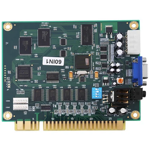
UGPCB provides Communication equipment printed circuit board assembly services. これは、上級業界の経験を持つPCBAワンストップアセンブリ工場です. お問い合わせへようこそ.


