高周波ハイブリッドスプリントには、ベースプレートが含まれています, 折り畳まれ、最初の内側のワイヤレイヤーに配置されます, 最初の外側のワイヤ層, はんだマスクインク層の上面が順番に下から上まで. The positioning circuit layer, the second outer wire layer, and the bottom surface of the substrate follow. The substrate includes a second layer of solder resist ink. The substrate comprises a high-frequency area and an auxiliary area; the auxiliary area is fixed, and the high-frequency area inlay should be positioned accordingly.
ユーティリティモデルは、高周波ハイブリッドスプリントを提供します, divided into two parts: 高周波エリアと補助エリア, providing mechanical support. 高周波エリアは独立して配置されており、高周波材料のみでできています. This minimizes the use of high-frequency board materials and reduces production costs while satisfying high-frequency signal requirements.
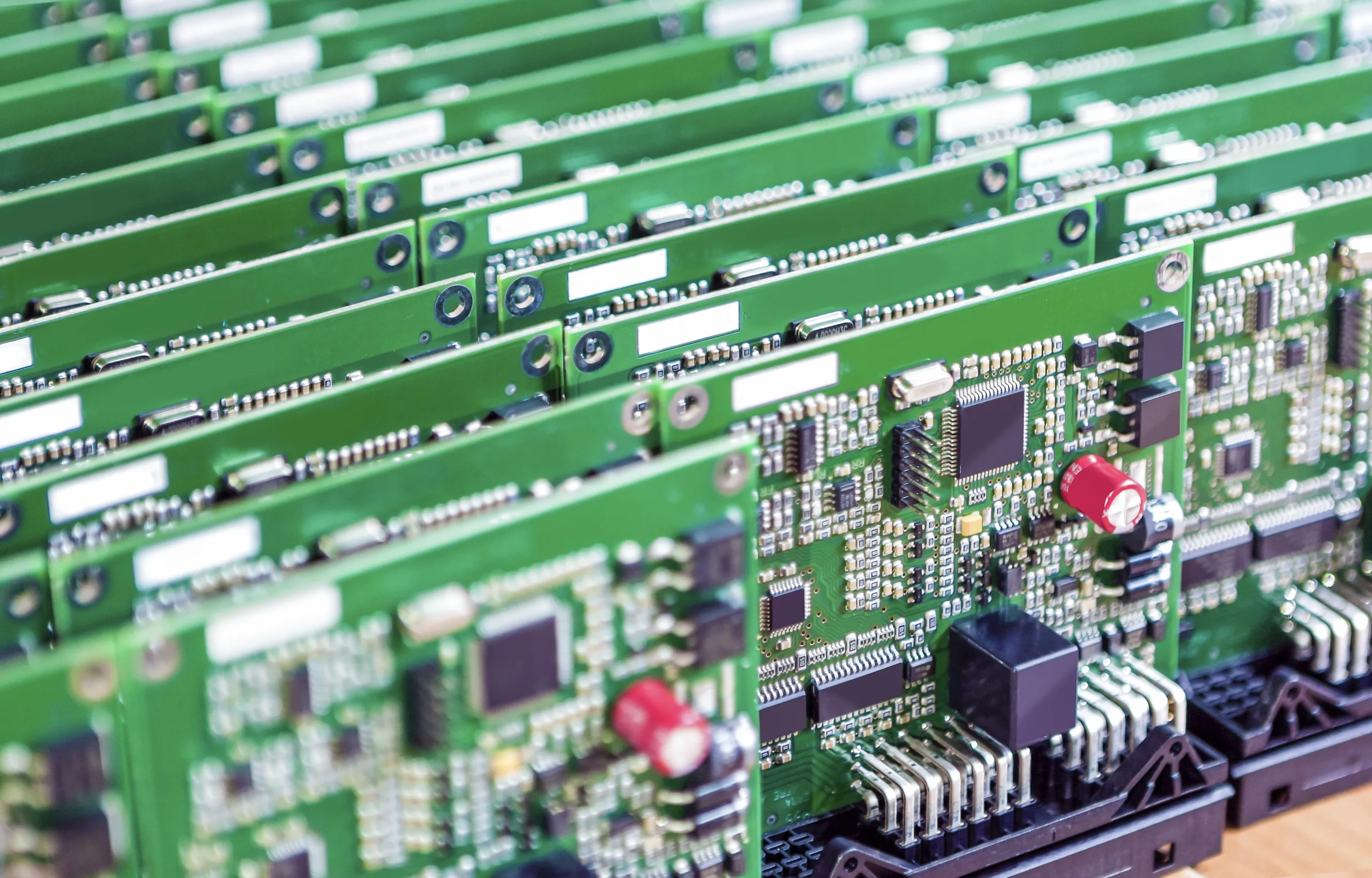
高周波ハイブリッド製品分類:
- レイヤー: 6
- 使用済みボード: RO4350B + FR4
- 厚さ: 1.6mm
- サイズ: 210mm x 280mm
- 表面処理: 金メッキ
- 最小開口: 0.25mm
- 応用: コミュニケーション
- 特徴: 高周波混合圧力
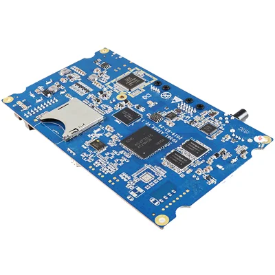
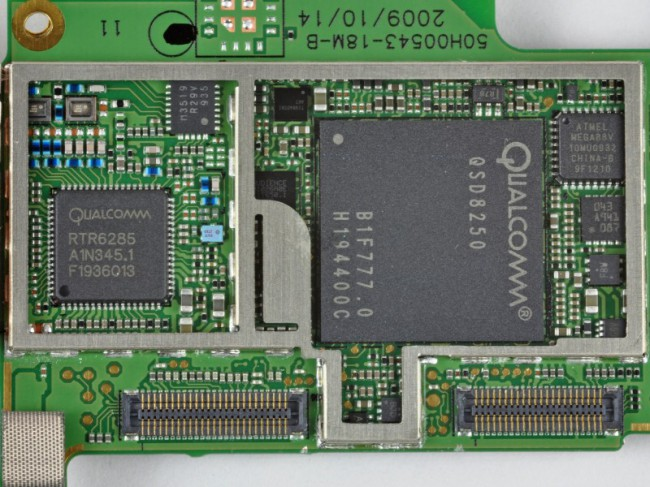
We provide Communication motherboard Turnkey PCB Assembly services. UGPCB is your one-stop Turnkey PCB Assembly company.


